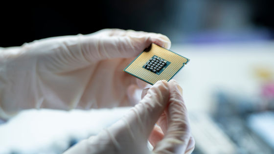
How to build your own RAM from scratch in your backyard to replace expensive memory modules.
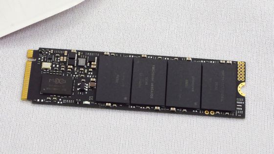
The increasing demand for AI has led to a surge in demand for memory (RAM) for GPUs, smartphones, and PCs. However, supply is heavily dependent on the three major companies Micron, Samsung, and SK Hynix, making it difficult to increase production immediately. In response, the YouTube channel Dr.Semiconductor has released a video in which they attempt to produce RAM themselves by converting a shed in their backyard into a cleanroom and building their own semiconductor manufacturing equipment, instead of waiting for a new factory to be built.
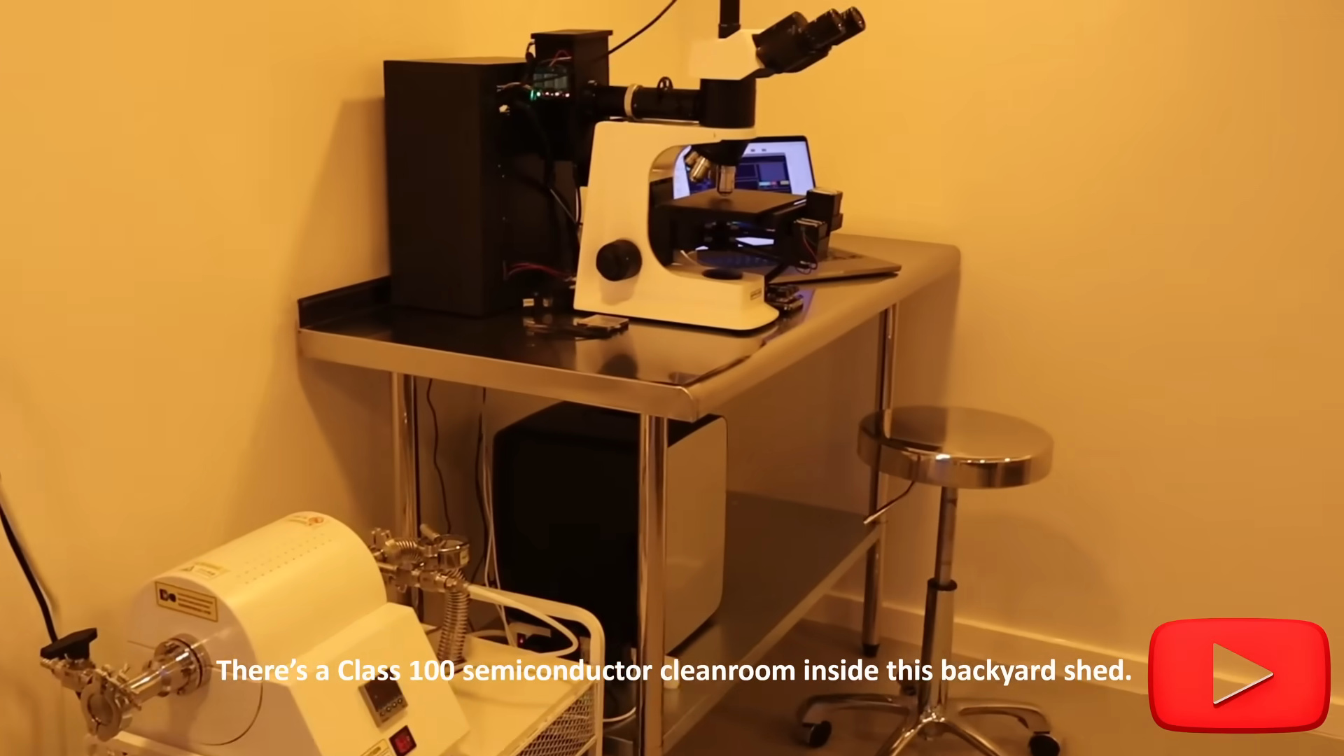
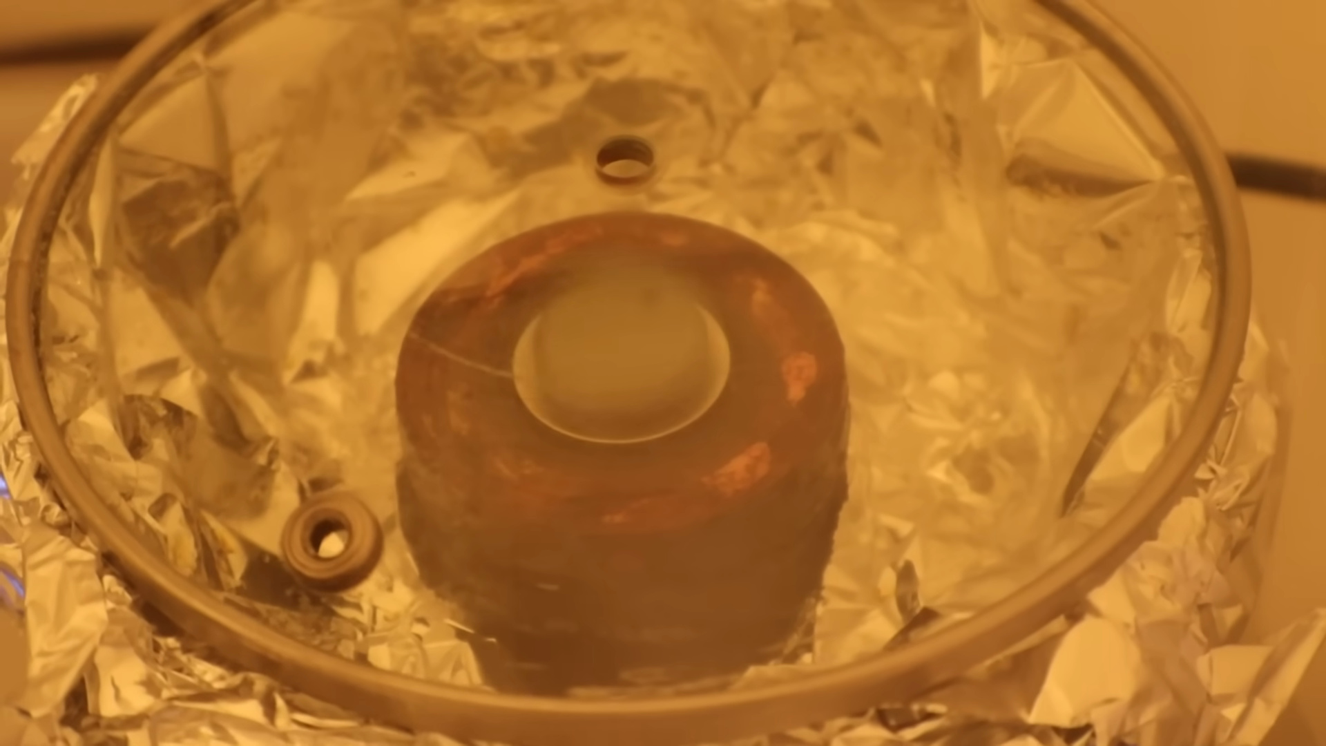
This is the shed in the backyard that I converted into a cleanroom.
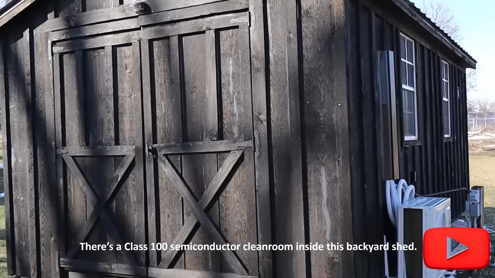
This cleanroom meets the Class 100 standard, which states that 'there are no more than 100 particles larger than 0.5 μm per cubic foot of air.'
Dr.Semiconductor has published the following information about building a cleanroom, so if you're interested in building a cleanroom at home, please refer to it.
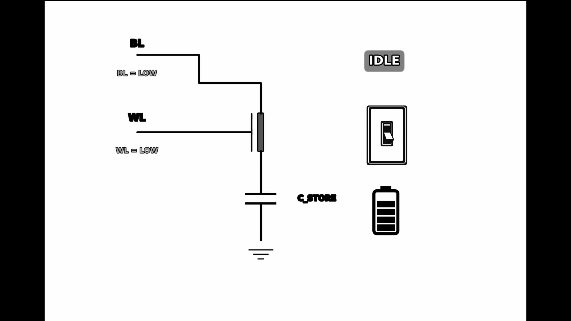
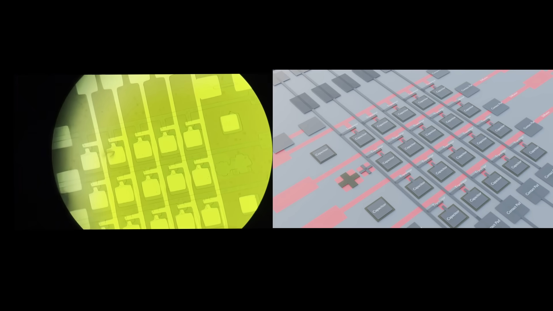
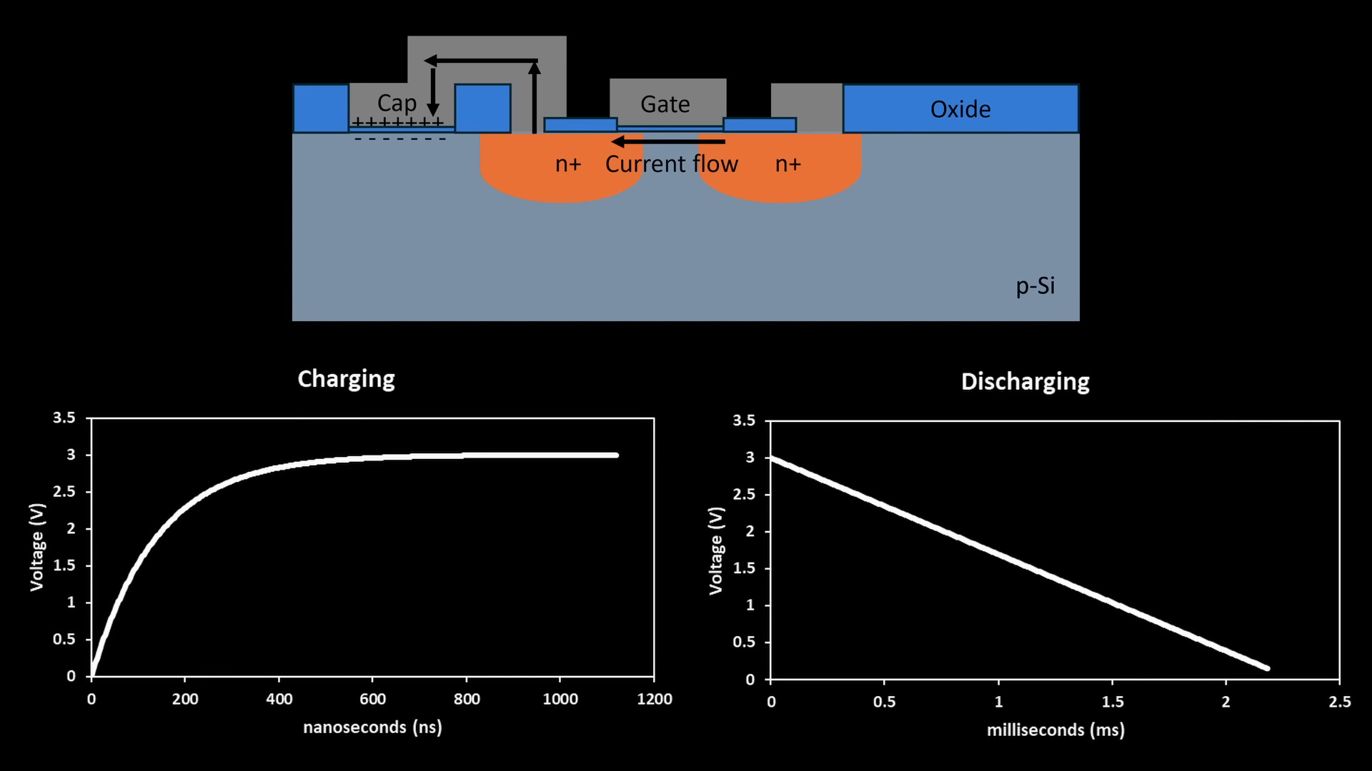
A RAM chip contains numerous cells arranged in a vast matrix, with one transistor and one capacitor at each intersection. The transistor acts as a switch, and the capacitor acts like a small battery that stores electricity. When the transistor is turned on, charge accumulates in the capacitor, allowing it to hold one bit of information. When reading the data, the transistor is turned on again, but this causes the charge to flow out and decrease, so periodic refreshing is necessary.
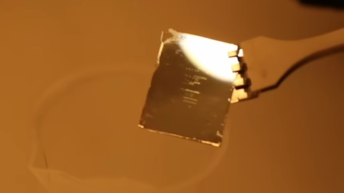
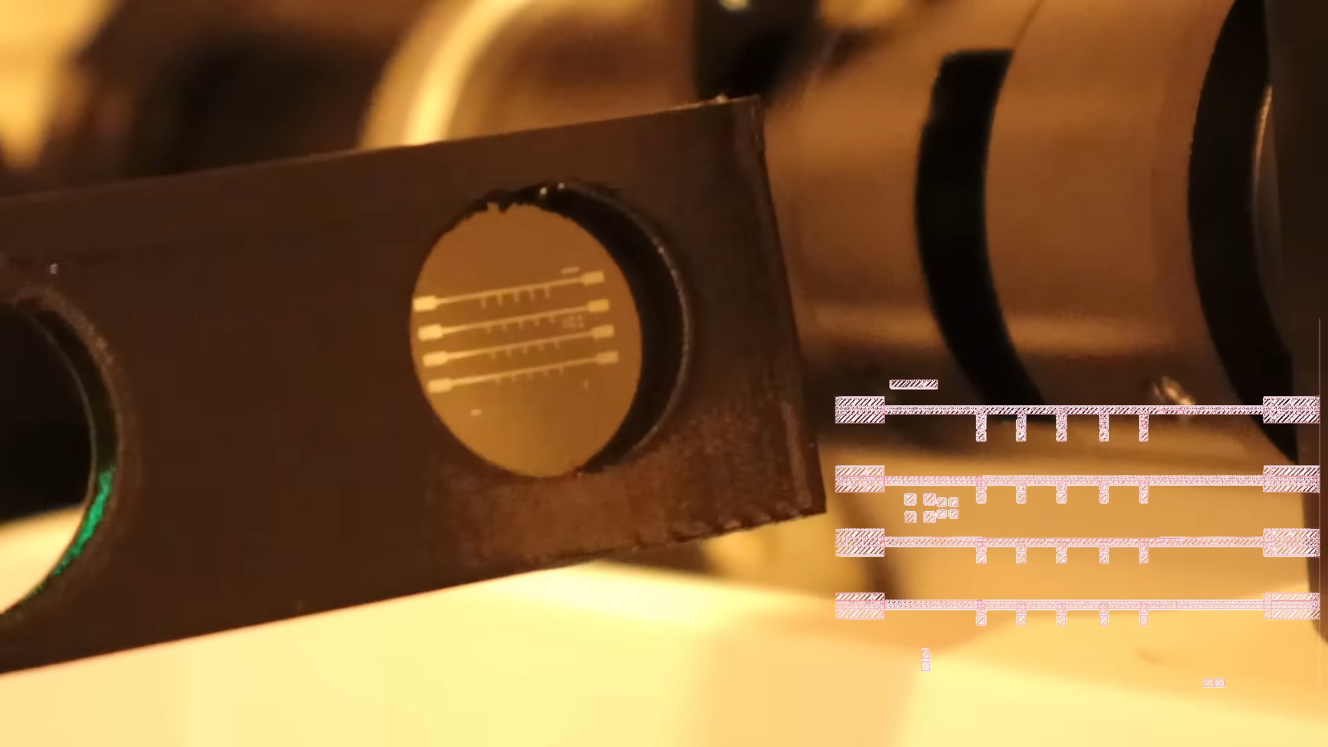
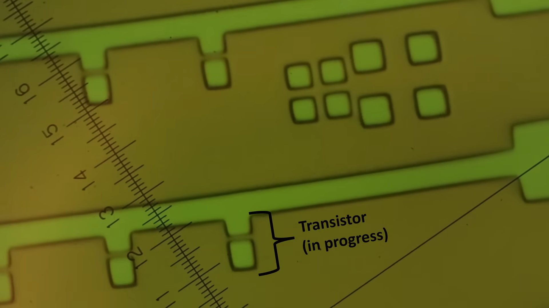
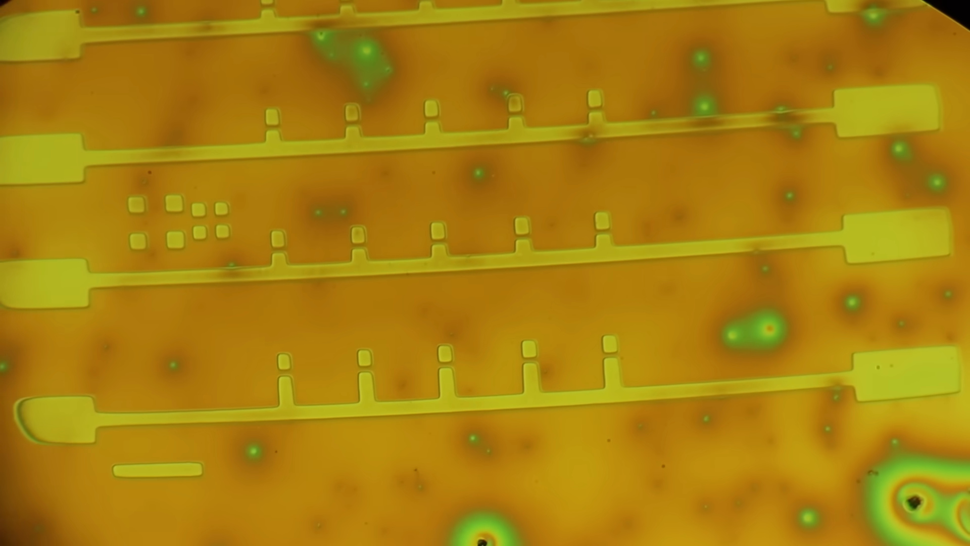
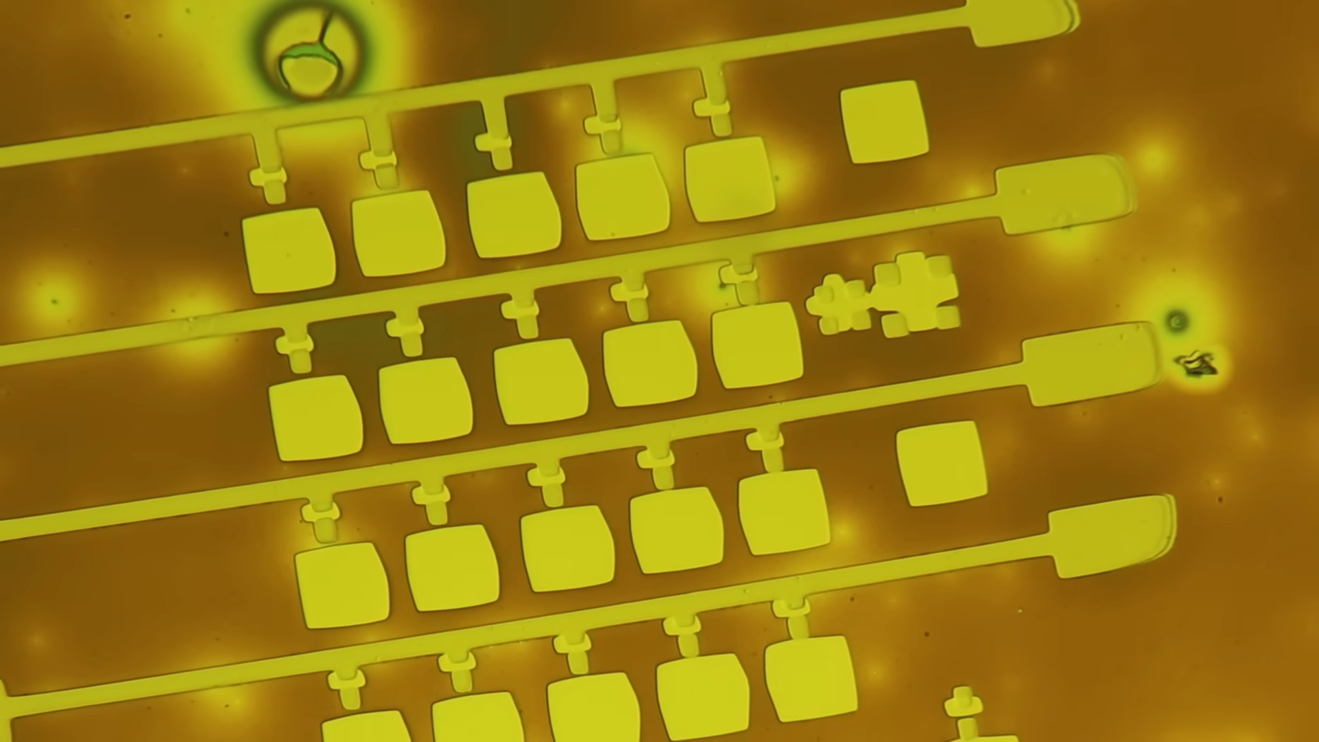
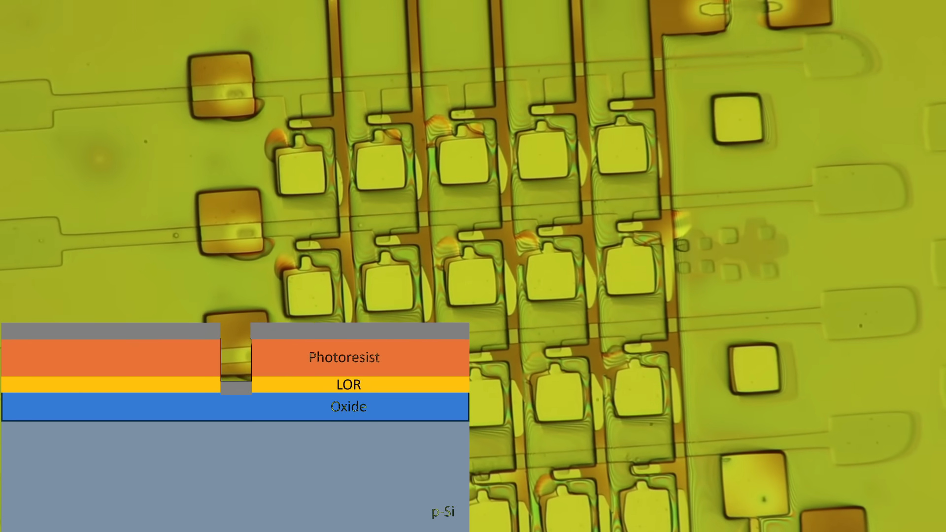
In the actual prototype, a small 5x4 memory array was designed. A transistor and a capacitor are placed at each intersection, with the final transistor gate length targeted at just under 1 μm. The different colors in the diagram indicate different processed layers; semiconductors are created by stacking these layers in sequence.

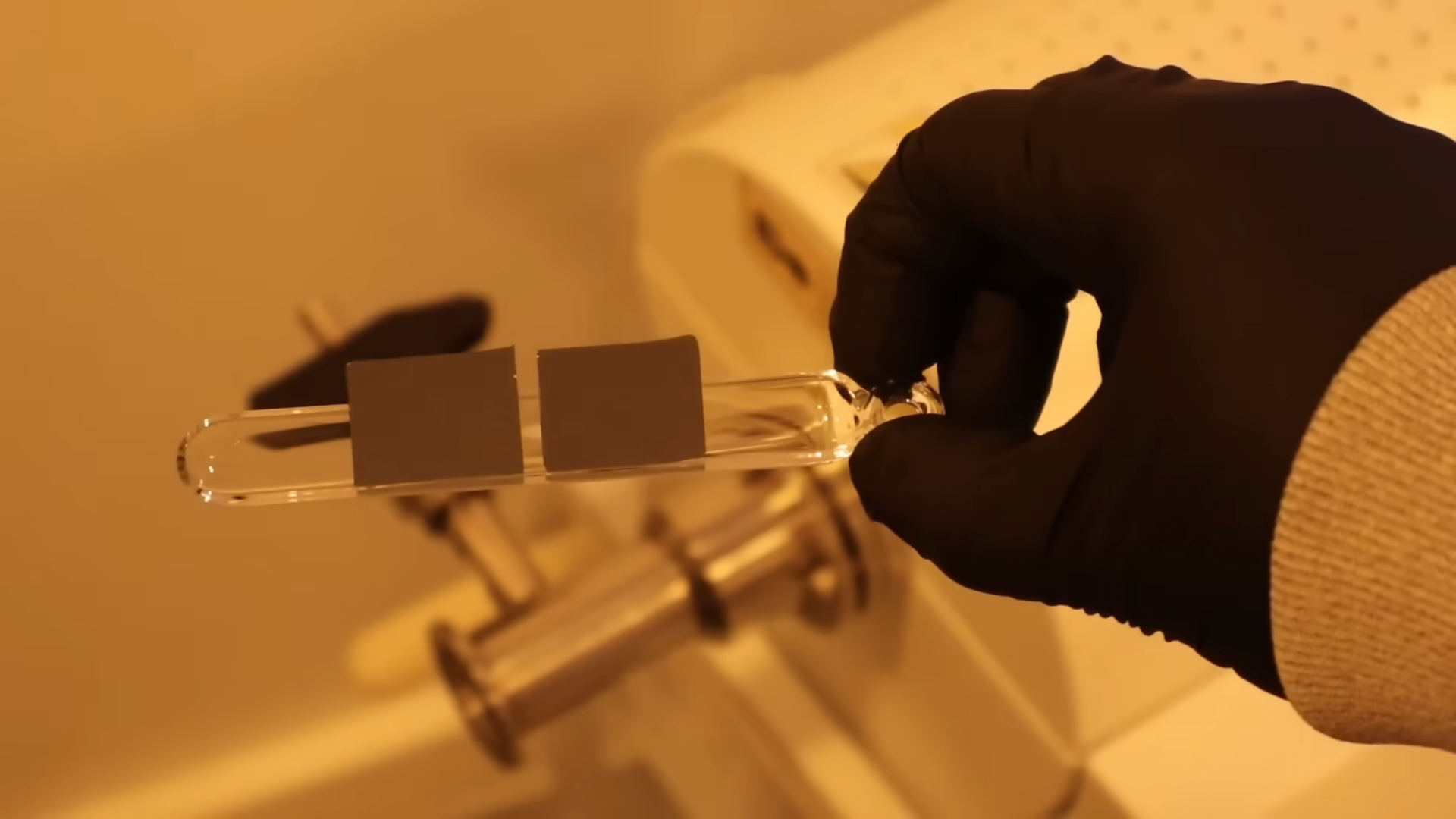
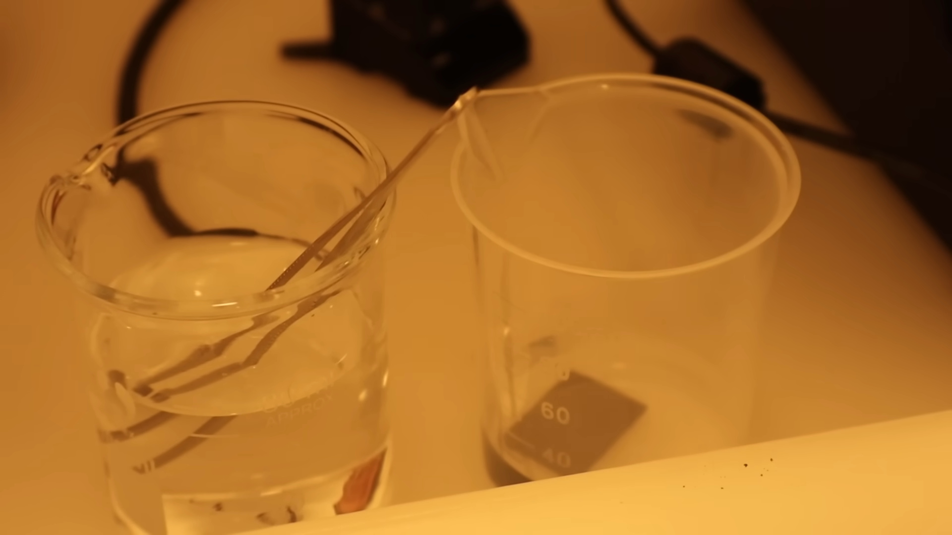
The material used is a silicon wafer. First, a large wafer is cut into small chip-sized pieces using a diamond scribing tool. Because silicon tends to break along the crystal orientation, it can be divided relatively cleanly.
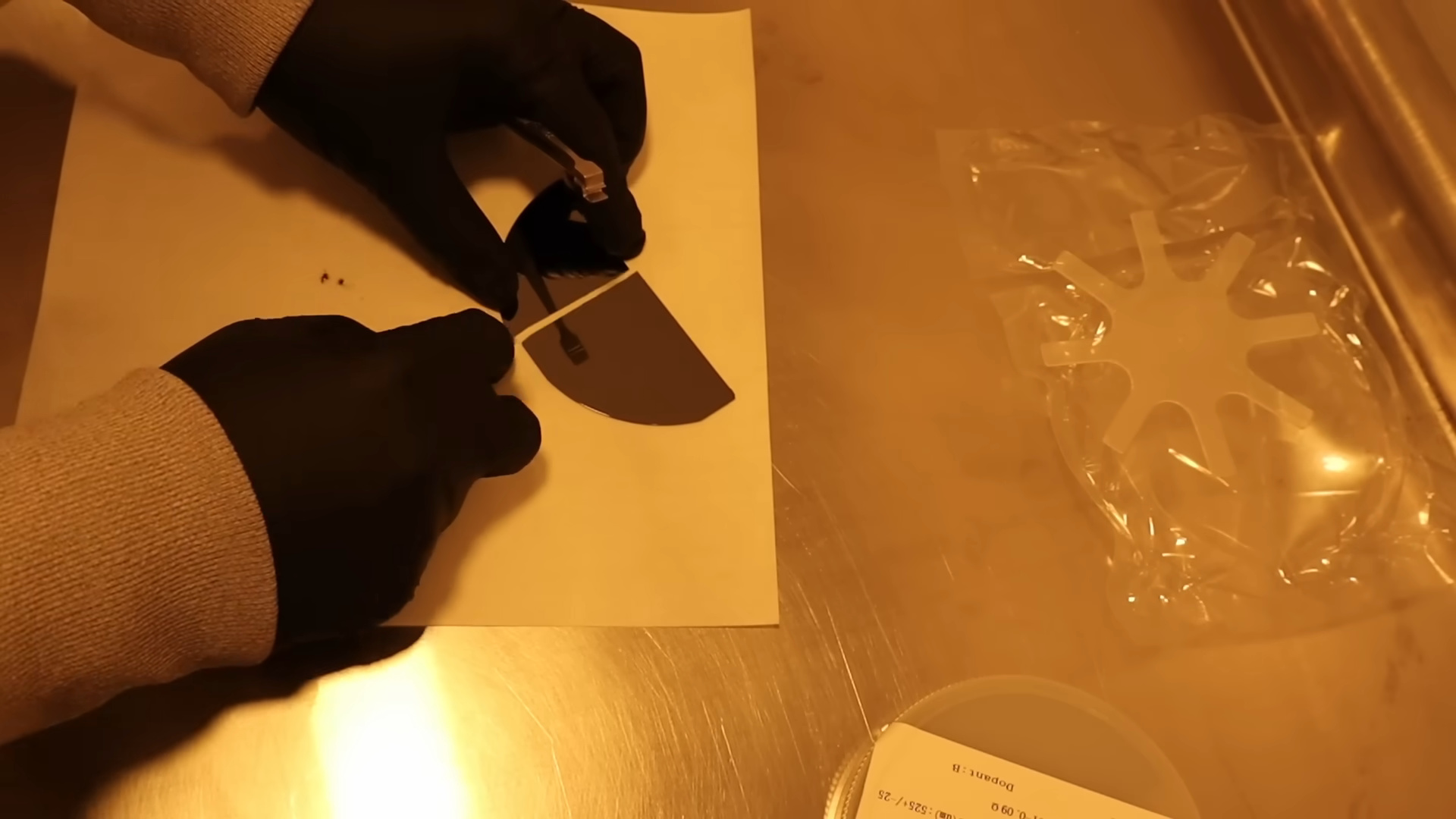
Afterward, the material is cleaned with acetone and isopropyl alcohol to remove any debris or organic matter from the cutting process.
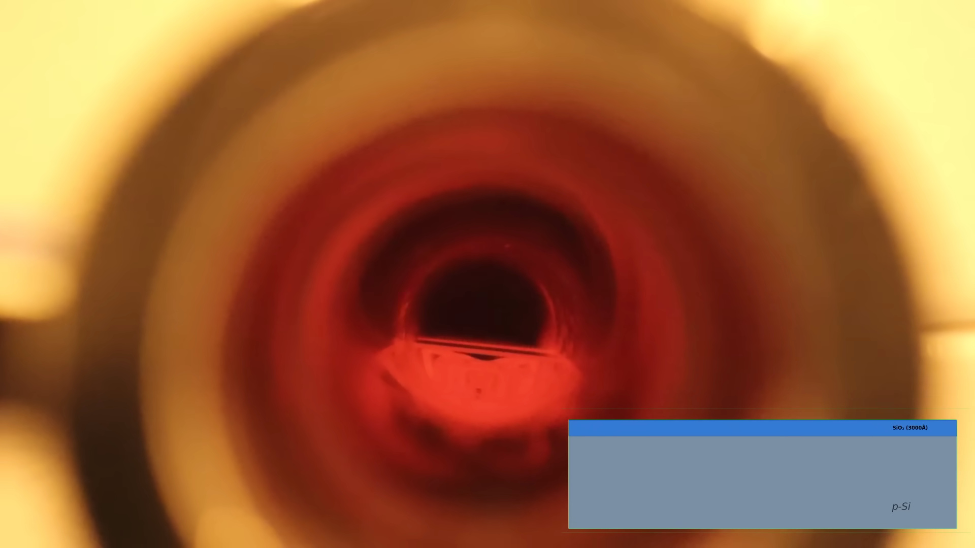
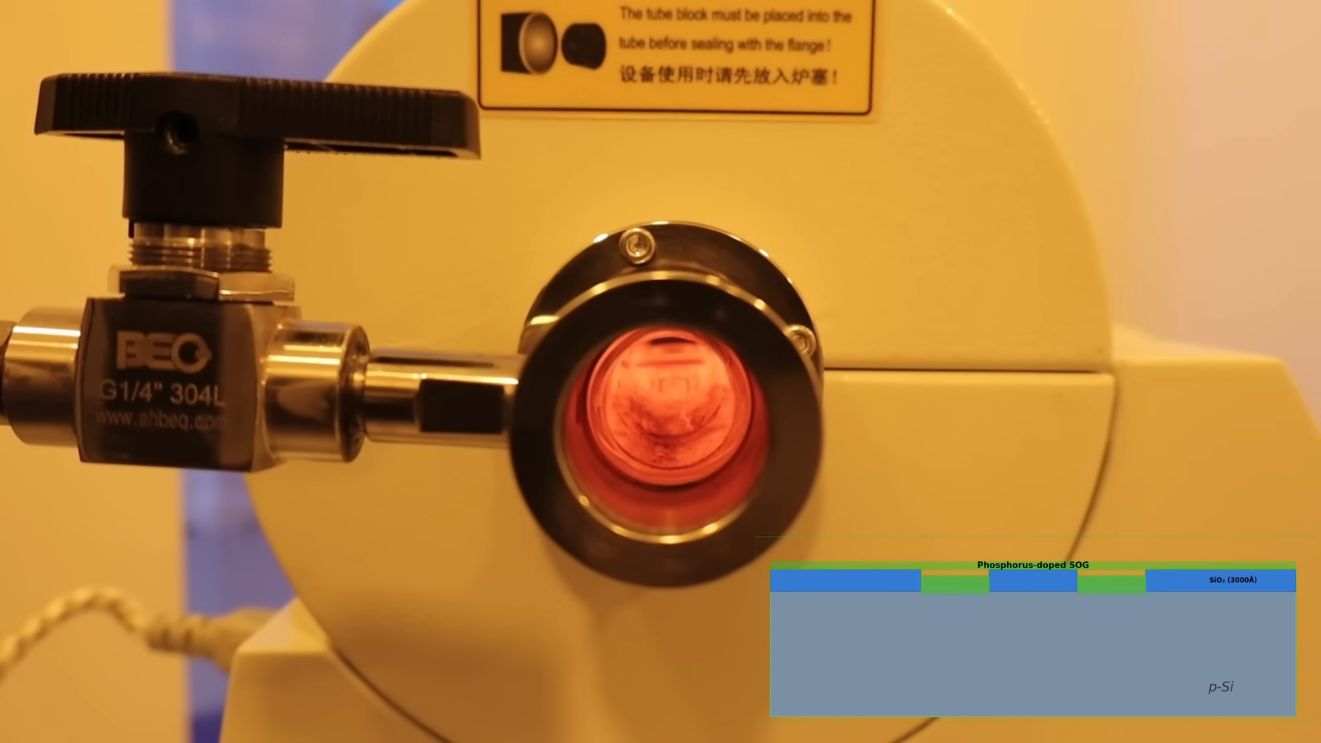
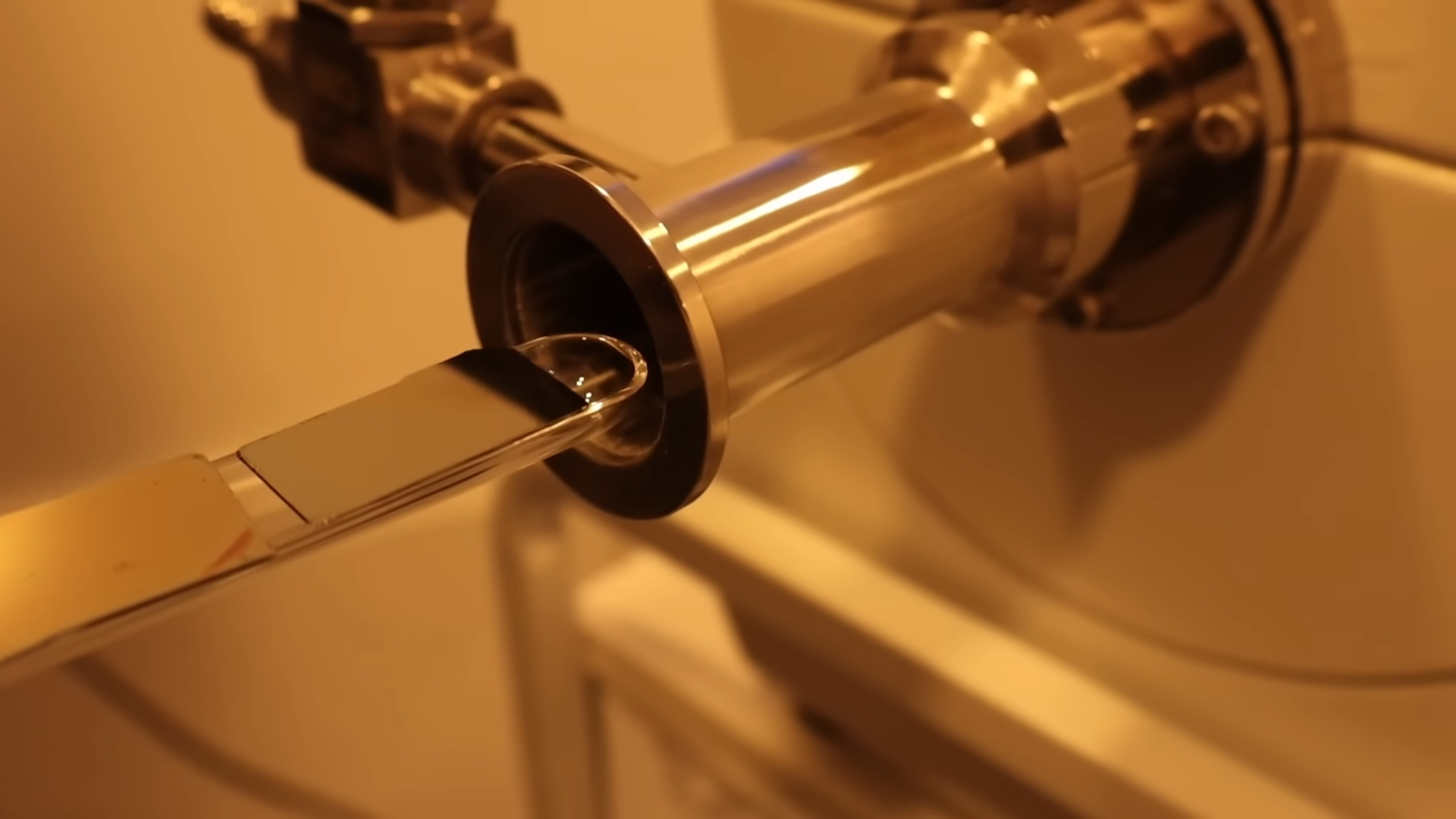
After cleaning, the silicon is placed in a furnace and oxidized at an extremely high temperature of 1100°C. This process transforms the silicon surface into an oxide film, or a glass-like film.
This firing process grows an oxide film approximately 3300 Å (angstroms) thick. This film is used in subsequent processes to protect the surface or as a mask to process only the necessary areas.
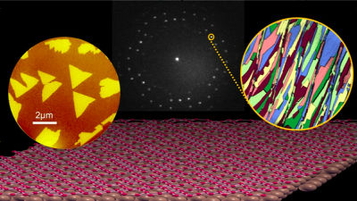
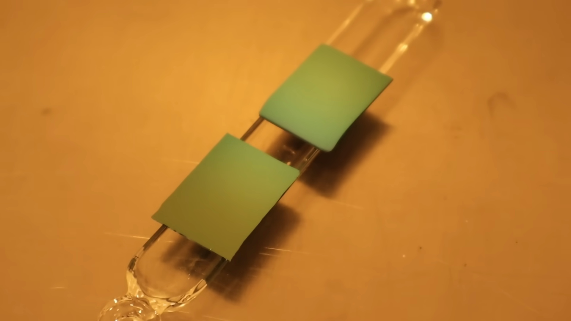
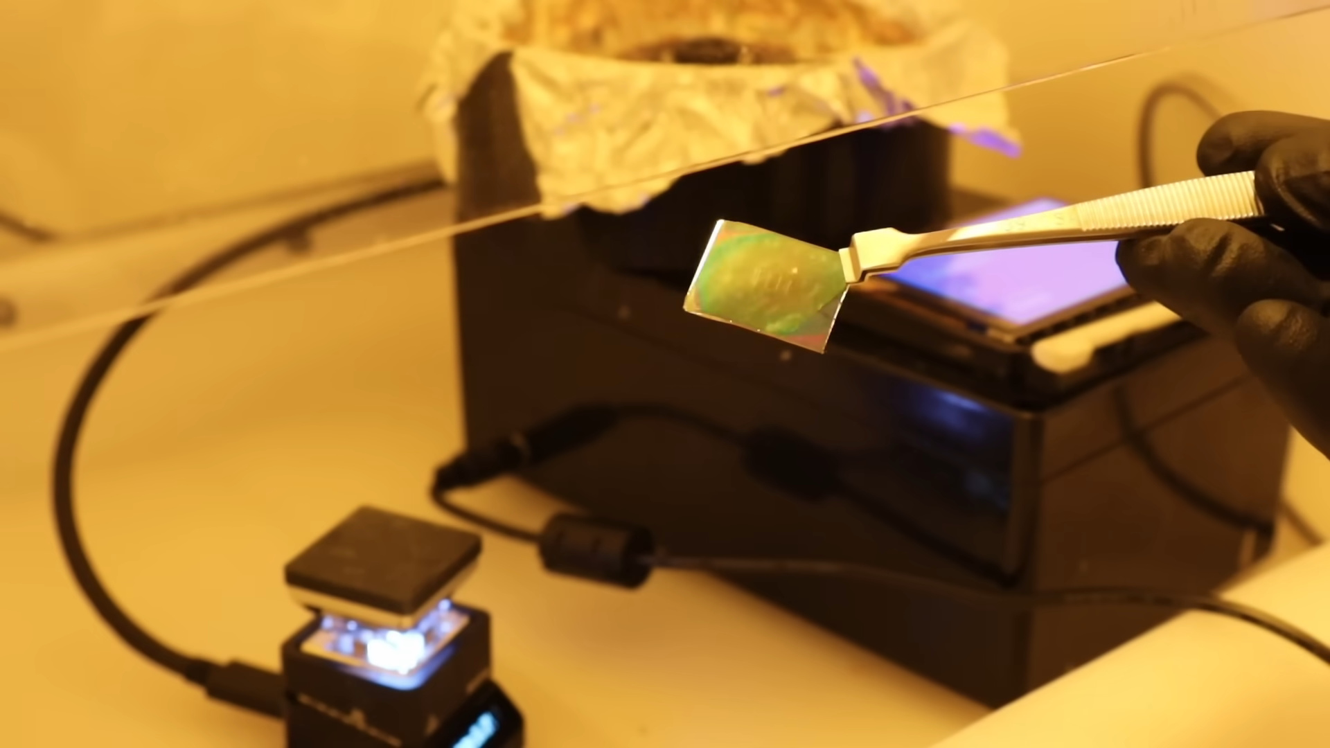
The silicon wafers turn a beautiful green color after firing.
First,
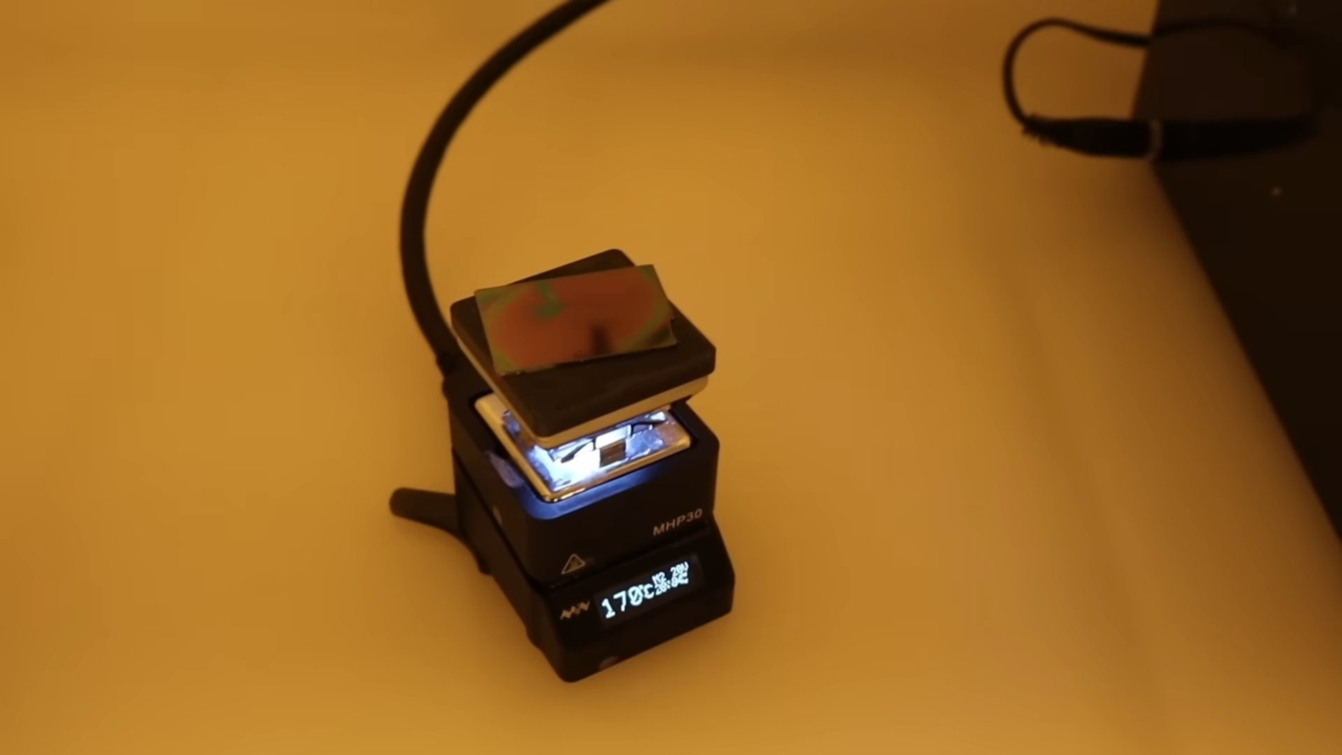
Next, a photosensitive photoresist is spin-coated on top and baked at 100°C. This creates a uniform resist film slightly over 1 μm thick on the surface.
Next, the process moves to photolithography, where ultraviolet light is applied through a mask. Only the light that passes through the openings in the mask reaches the photoresist, and the exposed areas dissolve and are removed in the developing solution.
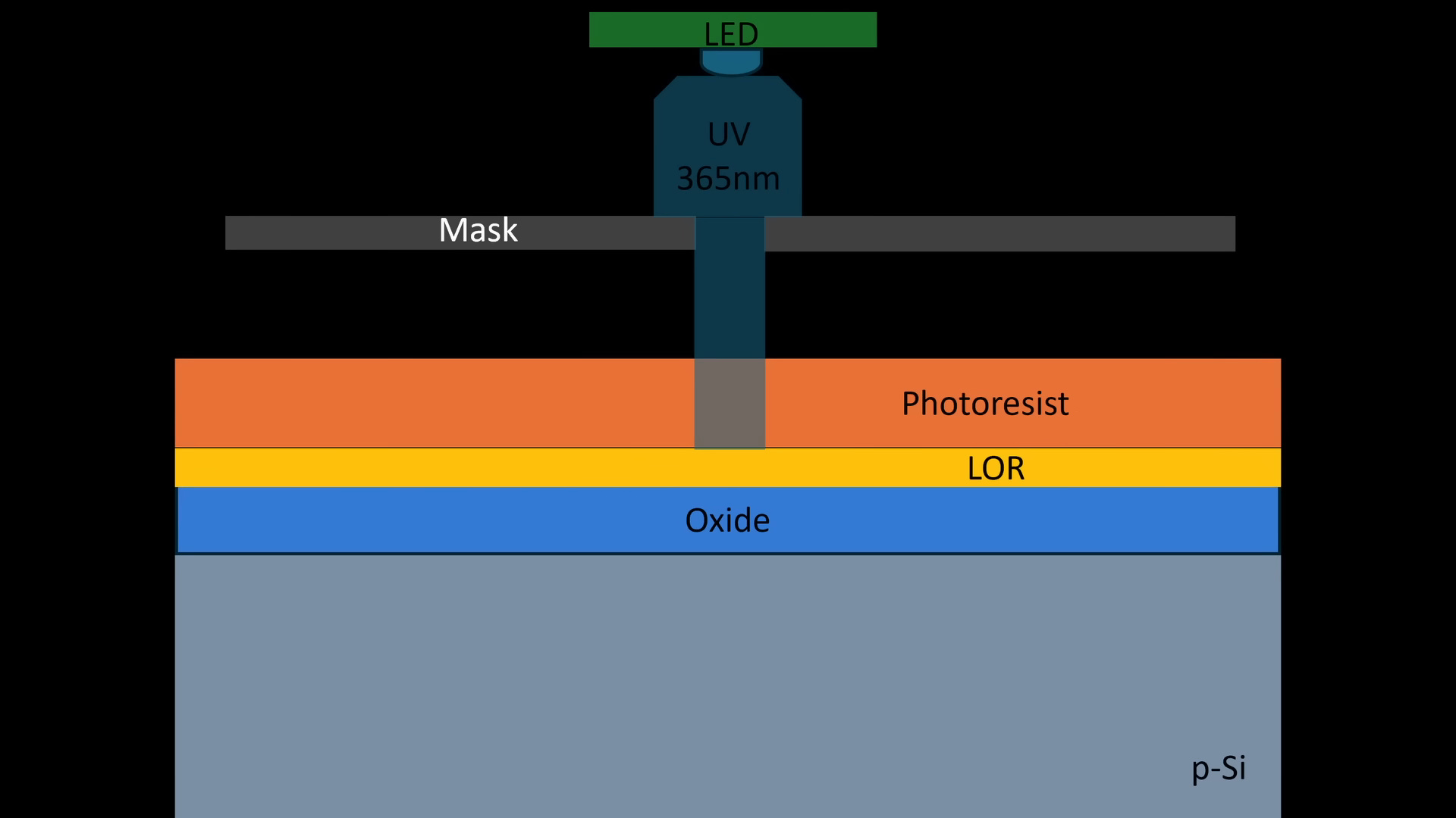
A microscope stepper is used to reduce and project the design pattern, transferring submicron-level shapes onto the chip. This leaves only the areas to be machined later exposed.
A patterned photoresist is used as a mask, and the oxide film is removed by dry etching. In other words, only the unwanted glass film is selectively removed, exposing the silicon surface underneath.
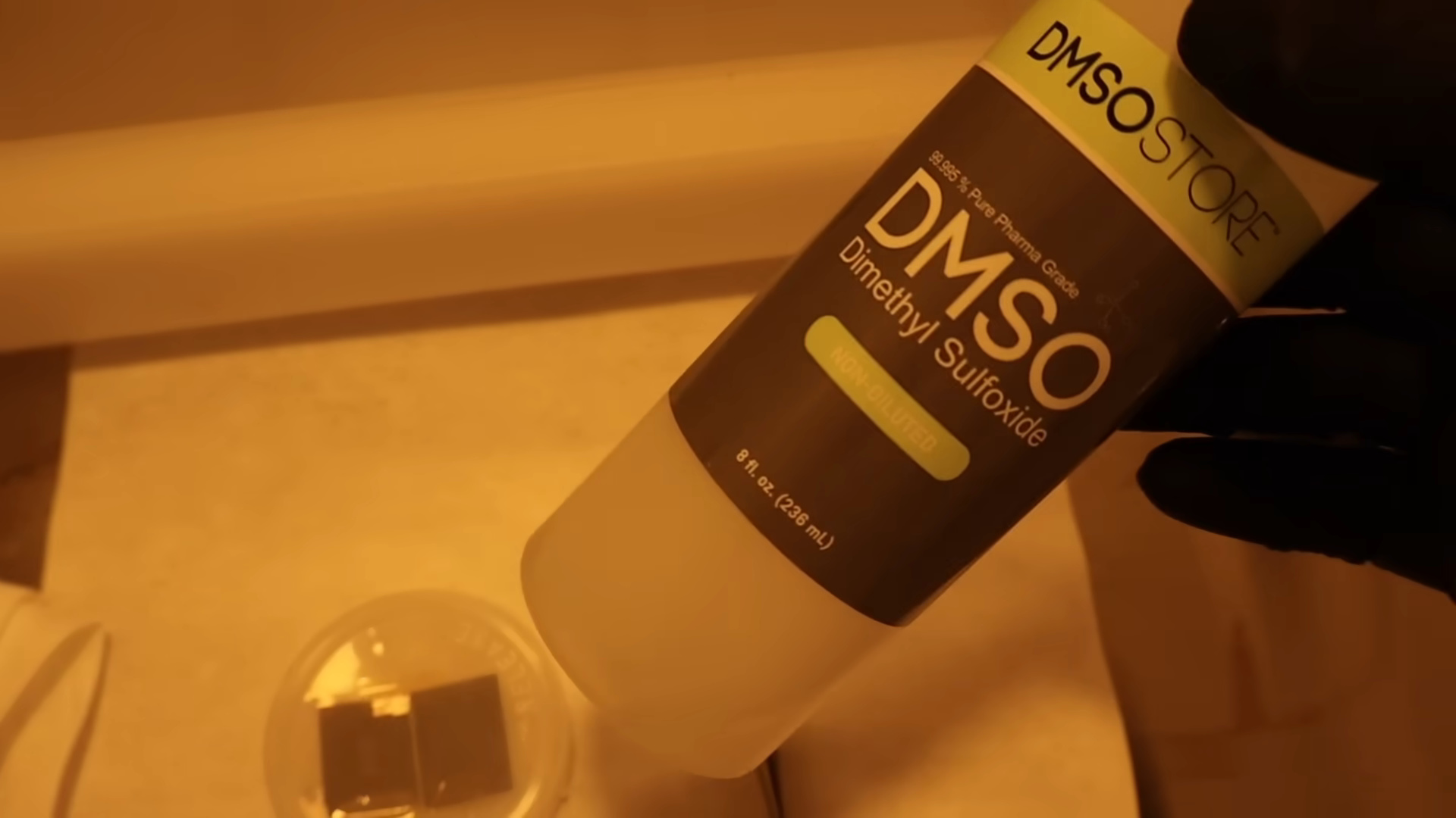
Once this process is complete, the photoresist itself is no longer needed and is removed with heated dimethyl sulfoxide (DMSO). As a result, a 'window' is created in part of the oxide film, allowing the next treatment to be applied only to that area.
Next is the process of creating the transistor's source and drain. The source and drain are the regions where the current enters and exits, and these need to be highly conductive.
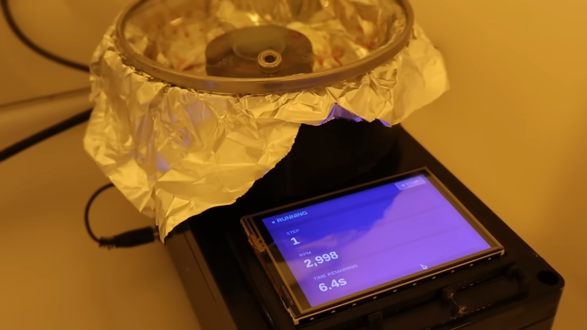
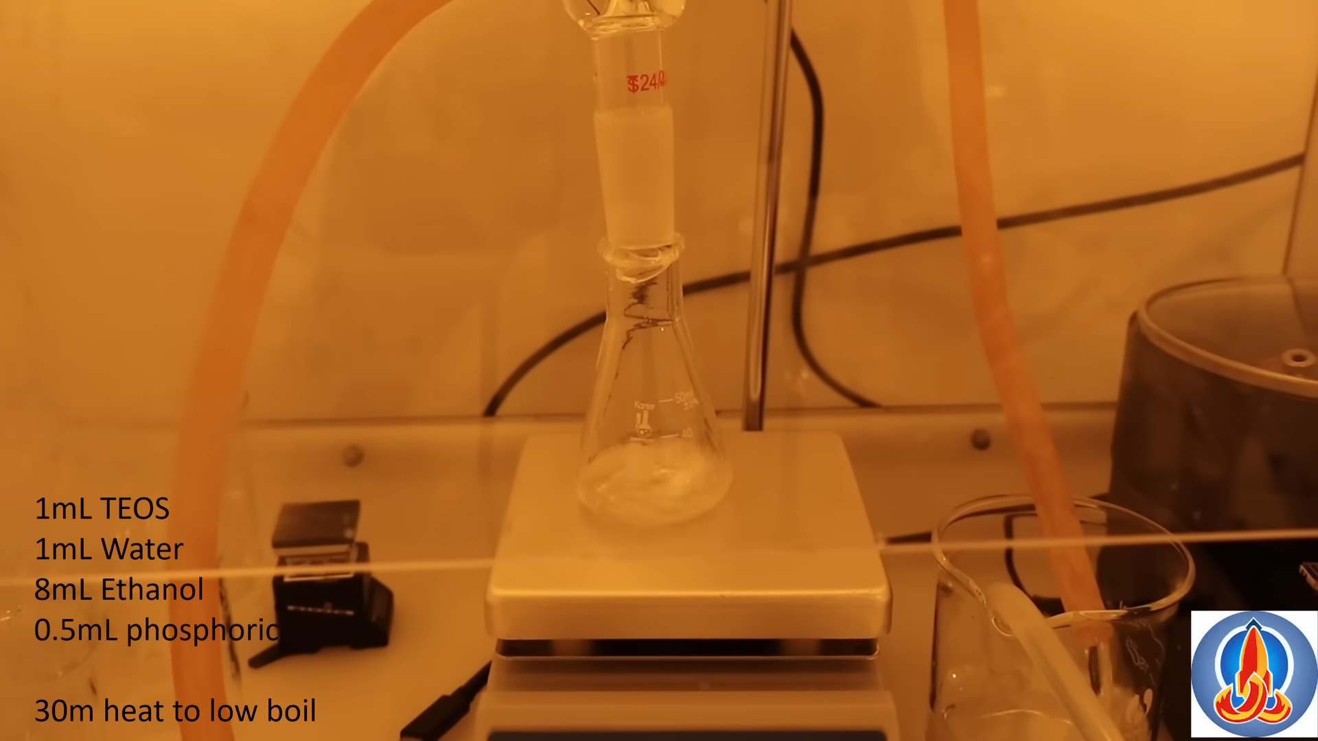
Therefore, phosphorus is added to the silicon through the open window to dope it. Normally, expensive equipment such as ion implantation is often used, but since this is being done in a clean room in a storage room, a method of applying the agent and diffusing it by spinning is adopted.
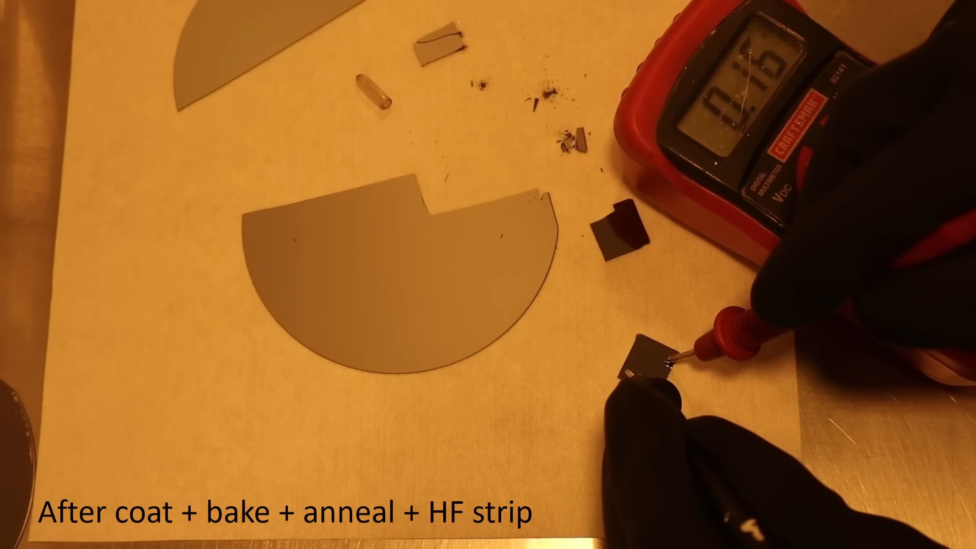
First, we verify the effect of this phosphorus-based material on a test specimen. The original wafer had high resistance, making it difficult to detect continuity with a tester, but strong conductivity was confirmed in the treated test specimen.
Therefore, phosphorus-containing spin-on glass was applied to the chips for the actual production run, and the temperature was gradually increased while baking. Although some glass deposits formed during the process, it was not considered a major problem.
Since the depth of doping is also important, the poster even built their own computer to calculate the phosphorus diffusion profile.

The goal is to create a conductive layer that is neither too shallow nor too deep. To achieve this, the phosphorus is first diffused by annealing at 1100°C for 5 minutes, then the spin-on glass is removed with hydrofluoric acid, followed by a further heat treatment at 1000°C for 10 minutes. This forms the source and drain layers.
Once the source and drain are formed, the next step is to create the channel region between them, that is, the transistor's switch itself. The LOR and photoresist are applied again, and this time, the image is carefully aligned to ensure proper positioning between the already formed source and drain before exposure. At the same time, the region for the charge-conserving capacitor placed on top of the transistor is also included in the exposure.
After development, hydrofluoric acid is used to remove the oxide film between the source and drain, as well as the oxide film in the area where the capacitor will be formed. The reason for thinning the oxide film here is to facilitate gate control in transistors and to increase the capacitance in capacitors. The channel region, in particular, is crucial for transistor operation, so it is treated as the most important part.
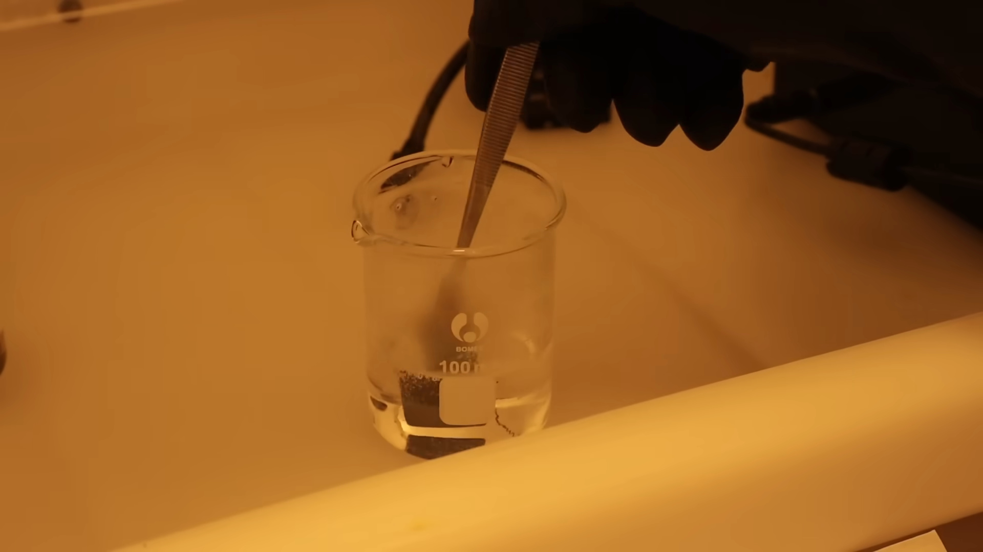
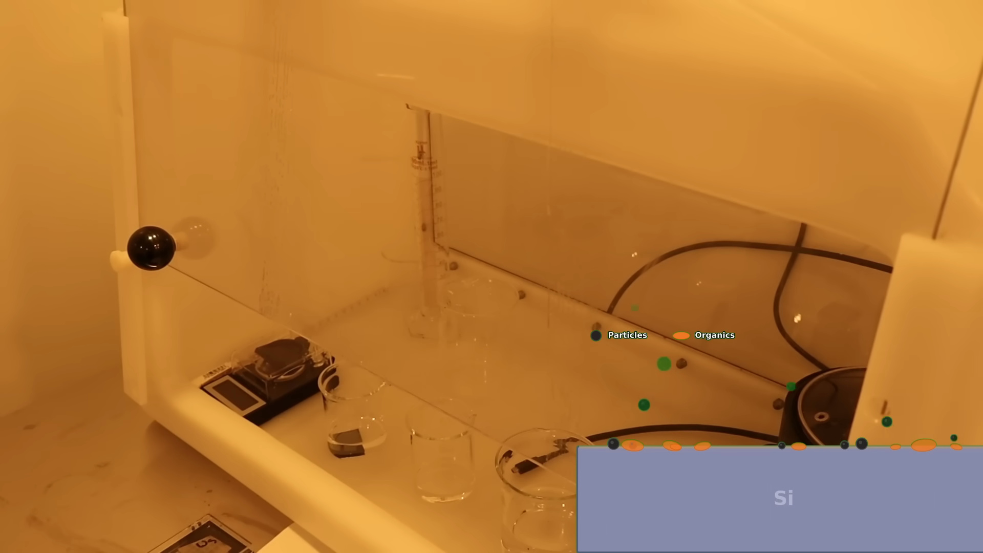
To clean the surfaces of critical parts, we perform a piranha wash here. This is a very powerful cleaning process that thoroughly removes organic matter and a lot of metallic contamination using a strong chemical solution.
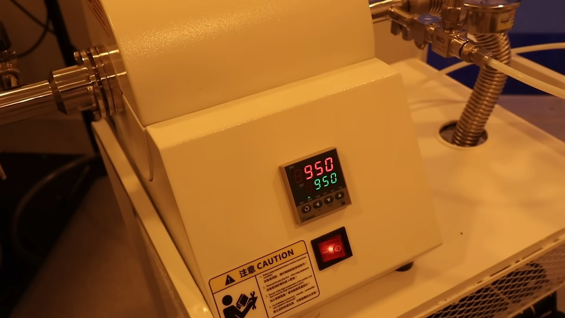
After thoroughly cleaning the surface, it is placed back into the furnace to grow a new oxide film.
The oxide film we will grow this time is considerably thinner than the initial protective film. By lowering the temperature to 950°C and processing for 38 minutes, we will create a gate oxide film and capacitor oxide film of approximately 200 Å, or 20 nm. This will improve the gate controllability of the transistor and make it easier to ensure sufficient capacitance for the capacitor.
On the other hand, a thick oxide film still remains on the outside of the device, while a thin oxide film is created only where necessary.
Next is the formation of contact holes for electrical connection. Since the entire surface is covered with an oxide film, metal wiring cannot be directly connected to the silicon as is. Therefore, LOR and photoresist are applied again, and the surface is exposed using a contact-cutting mask to create small openings. Hydrofluoric acid is then applied to these openings to remove the oxide film only where necessary, creating a passage through which the metal can later make contact.
The final major step is metal wiring. Here too, LOR and photoresist are applied and the final mask is exposed, but this time, unlike the previous step, instead of cutting away the material, the resulting opening is used as a 'mold'.
In other words, this process uses the holes in the resist created so far as a stencil, and then sprays metal onto them. In practice, aluminum is deposited using a sputtering machine, and argon ions are used to strike a metal target, causing the ejected aluminum atoms to accumulate on the chip surface. This results in metal adhering to the entire surface, but only the areas corresponding to the openings in the resist are needed.
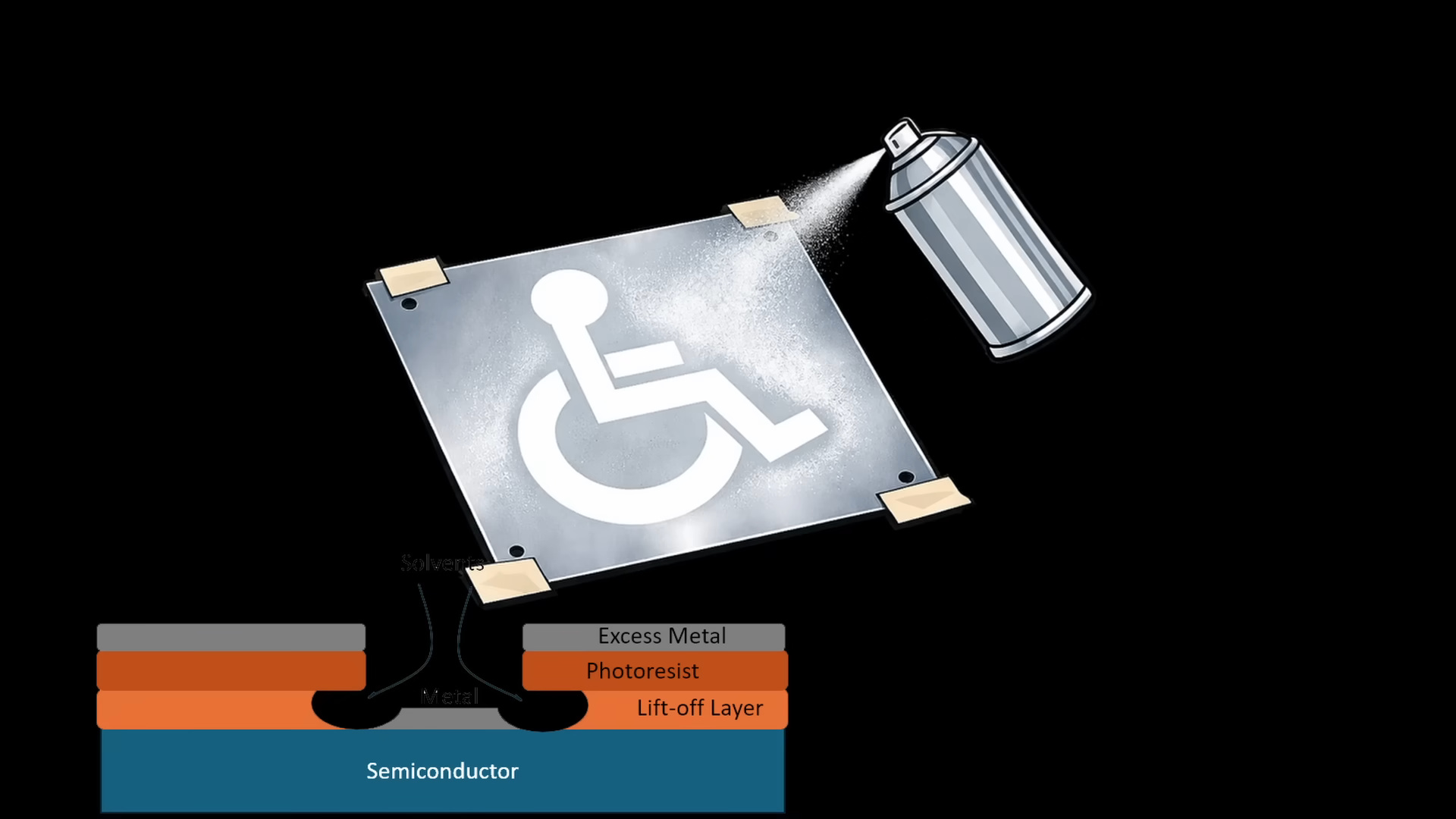
Then, it is immersed again in heated DMSO to remove the excess metal along with the resist. This is called lift-off.
When viewed under a microscope after lift-off, it can be seen that the transistors, capacitors, and various connecting wires are complete. In terms of cross-sectional structure, there is a silicon substrate at the bottom, with the source and drain and a thin oxide film on top, and then the aluminum gate electrode and capacitor electrodes on top of that. With this, the basic structure of a DRAM cell, in which the transistor controls the current and stores charge in the capacitor, has actually been created.
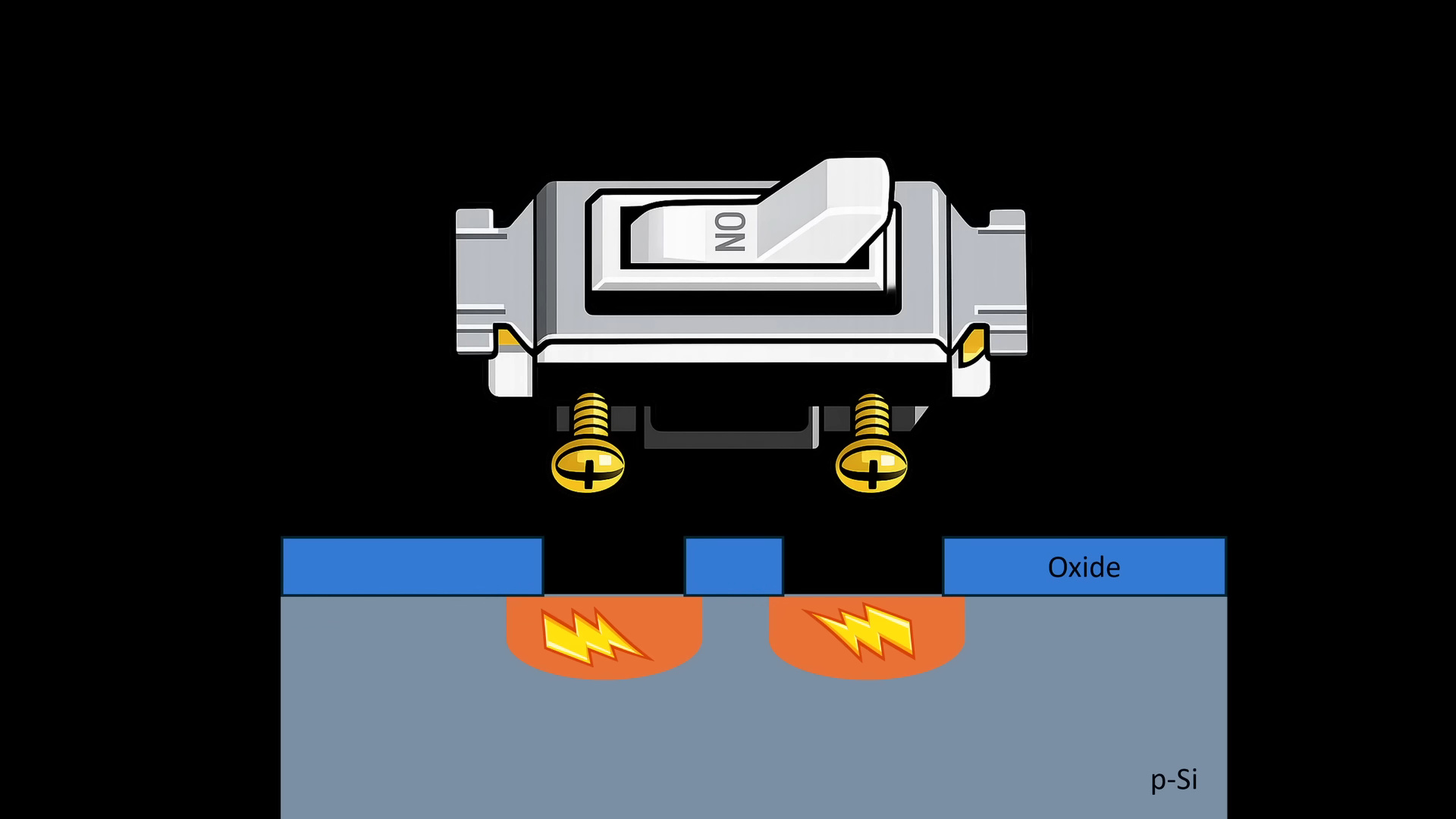
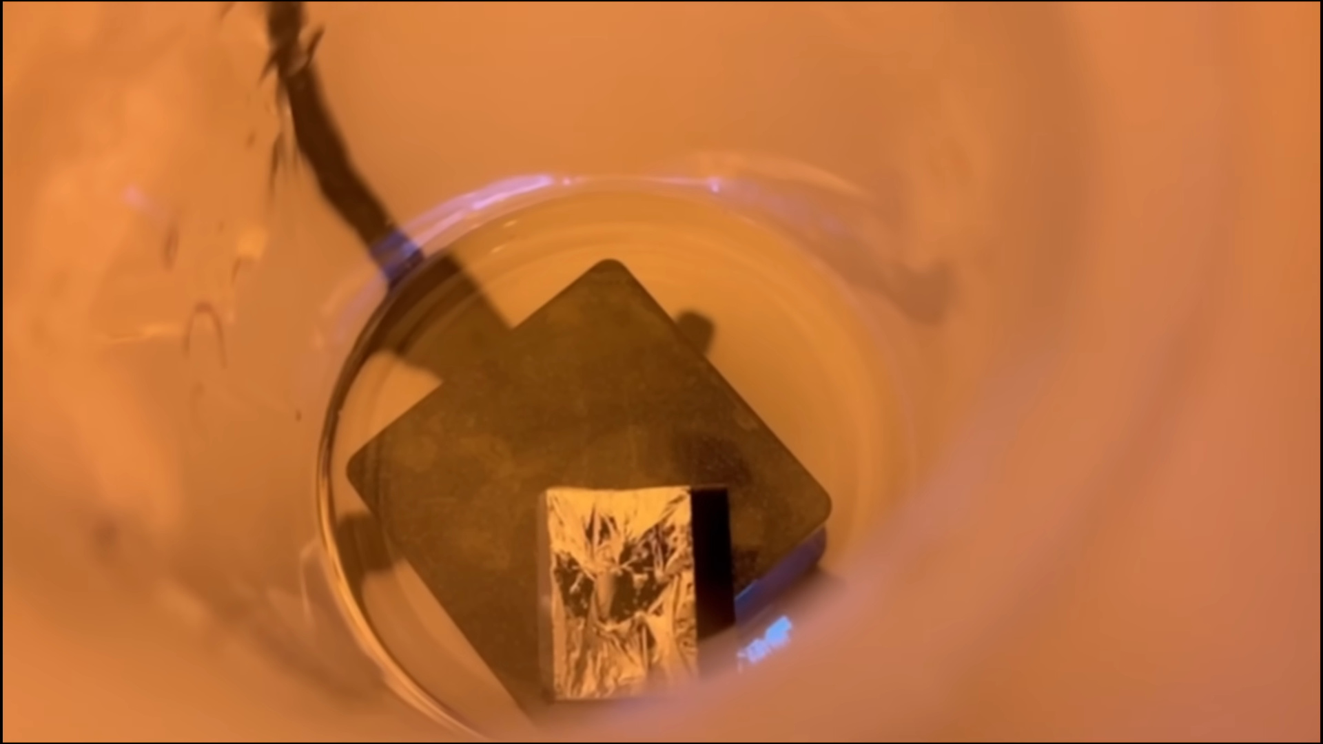
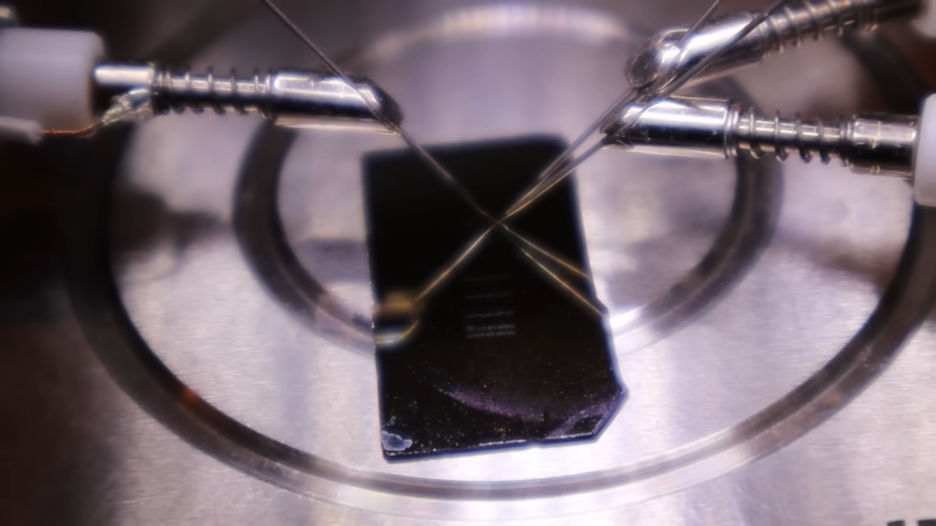
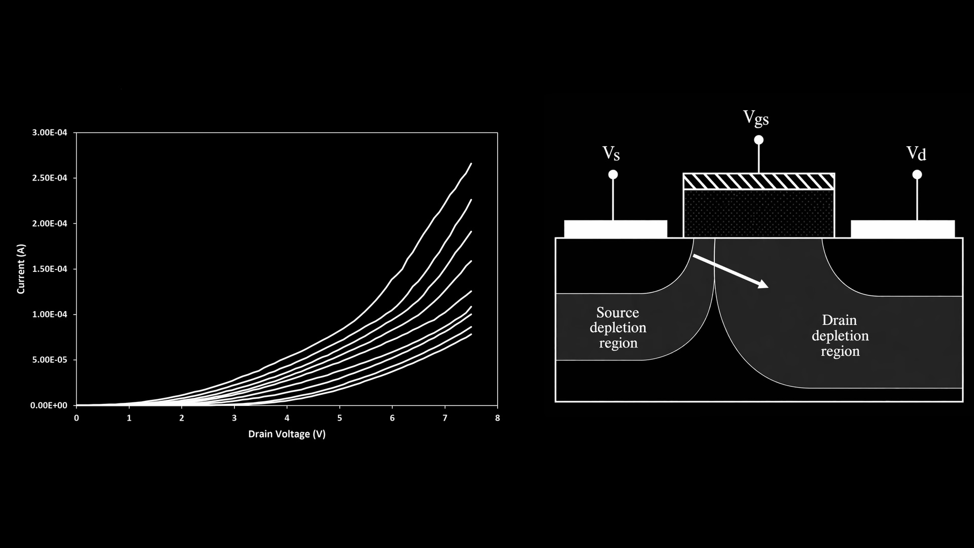
Now we move on to measurements. Since these are nanoscale elements, we cannot connect them with ordinary wires, so we use a micro-manipulator to apply a tiny probe needle for measurement. In the transistor measurements, we can confirm that the current flowing through the transistor changes depending on the gate voltage, confirming that it functions as a switch. We can observe not only complete digital on/off behavior, but also behavior that allows for continuous change in output.
However, the transistor characteristics were not ideal, and a problem was observed where the current continued to increase at high voltages. This is because the distance between the source and drain is short, less than 1 μm, so when a high voltage is applied, the influence regions of the two connect, and the gate control becomes weak. Although it can be used as long as it is operated at low voltages, this illustrates the difficulty of miniaturization.
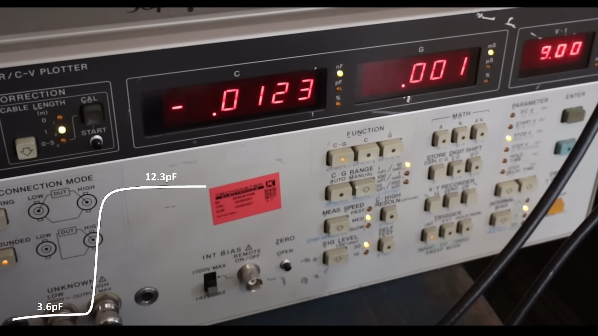
Next, the capacitor itself was measured. The capacitance was read while varying the voltage using a CV plotter, and the maximum capacitance was reported to be 12.3pF. This is quite close to the ideal value in the design, indicating that the target capacitor was successfully created.
When a transistor and a capacitor are combined as a single DRAM cell, it is confirmed that the transistor can quickly charge the capacitor to 3V in a few hundred nanoseconds. After that, the capacitor voltage gradually decreases and is almost lost in just over 2ms. In other words, data can be retained, but a refresh at a fairly short period is necessary. Although this is shorter than the 64ms or more retention period of commercially available DRAM, it is a successful demonstration of the operating principle for a home-built project.
Dr.Semiconductor boasts that the DRAM they created is 'the first RAM ever made at home.' However, they currently only have a few cells and it's not yet a practical memory chip. Dr.Semiconductor stated that their next goal is to arrange many of these cells to create a large array and eventually develop it to a level where it can be connected to a PC and used.
Related Posts: