A gap the size of a single atom is a barrier to next-generation semiconductor development.

Research at Vienna University of Technology has revealed that two-dimensional materials, which are expected to be used in next-generation ultra-small computer chips, may face unexpected limitations in actual devices. The problem lies in the atomic-level gaps that form between the material and the insulating layer. Although these gaps are extremely small, at approximately 0.14 nanometers in size, they can hinder further miniaturization of semiconductor devices.
Device-scaling constraints imposed by the van der Waals gap formed in two-dimensional materials | Science
The hidden atomic gap that could break next-generation computer chips | ScienceDaily
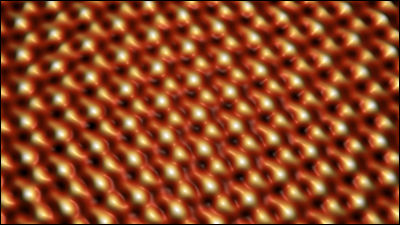
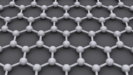
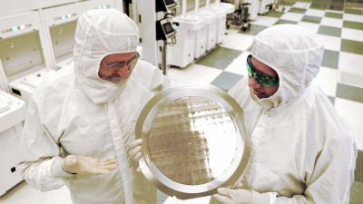
In recent years, 'two-dimensional materials' such as graphene and molybdenum disulfide have attracted attention as next-generation semiconductor materials. Two-dimensional materials are only about one to a few atoms thick, and it is thought that they have the potential to make transistors even smaller and more efficient.
A typical transistor has a gate electrode that controls the on/off state of the current. The gate electrode does not directly pass current through the semiconductor material, but rather controls the state of electrons in the semiconductor by applying an electric field with an insulating layer in between. Therefore, the insulating layer not only blocks the current, but also efficiently transmits the electric field of the gate electrode to the semiconductor layer.
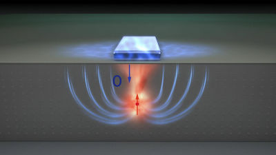
However, when a two-dimensional material is combined with an insulating layer, the two materials are weakly in contact, mainly due to van der Waals forces , creating an atomic-level gap at the interface called a 'van der Waals gap.' This gap is about 0.14 nanometers wide, smaller than the distance of a single sulfur atom, but it has an electrical effect that cannot be ignored.
This van der Waals gap acts as a 'tunneling barrier' for electrons passing through through quantum mechanical tunneling , and in some ways reduces the current leaking from the gate electrode to the semiconductor layer. However, at the same time, this gap also acts as an extra layer of low dielectric constant, weakening the capacitive coupling between the gate electrode and the two-dimensional material. In other words, even if you try to improve gate control by thinning the insulating layer, as long as this gap remains at the interface, it will appear electrically as if an extra thickness has been added.
Glasser et al. explain that this gap increases the equivalent oxide film thickness, an indicator of the electrical thinness of the gate insulating layer, by approximately 0.27 nm. While this is a small difference at the atomic level, it has a significant impact on semiconductor devices that have been miniaturized to the extreme. Even if the material itself has excellent properties, the mere presence of this gap at the interface with the insulating layer can weaken gate control and potentially limit performance improvements.
Glasser et al. quantified the impact of gaps on device miniaturization and showed that even with excellent material properties, gaps remaining at the interface may prevent the level of miniaturization required for future semiconductors from being achieved. Glasser et al. point out that 'as long as gaps exist, a fundamental limit will be reached.'
Glasser et al. have instead proposed 'fastener materials' as a solution. This idea involves creating a stronger interface where the two-dimensional material and the insulating layer are bonded together, rather than simply being weakly connected by van der Waals forces, thereby eliminating the problematic van der Waals gap itself.
Glasser and his colleagues state that 'if we focus solely on the material itself without considering the unavoidable problem of the insulating layer, we risk making a wrong investment in a technology with fundamental physical limitations.'
Related Posts: