TSMC unveils process technology roadmap through 2029, announcing A12, A13, and N2U, while A16 is postponed to 2027.
by
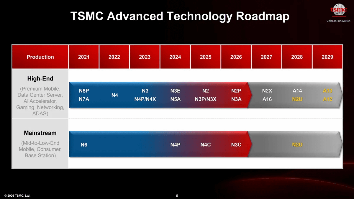
At its North America Technology Symposium 2026, held on April 22, 2026, TSMC presented a new semiconductor process roadmap looking ahead to 2029. The core of this roadmap includes the A13, a scaled-down version of the A14 ; the A12, which introduces backside power supply for AI and high-performance computing (HPC); and the N2U, an extended version of the 2nm generation. In addition, TSMC also unveiled technology plans for advanced packaging, automotive applications, and display drivers.
TSMC Debuts A13 Technology at 2026 North America Technology Symposium
https://pr.tsmc.com/english/news/3302
TSMC unveils process technology roadmap through 2029: A12, A13, N2U announced, A16 slips to 2027 | Tom's Hardware
https://www.tomshardware.com/tech-industry/semiconductors/tsmc-unveils-process-technology-roadmap-through-2029-a12-a13-n2u-announced-a16-slips-to-2027
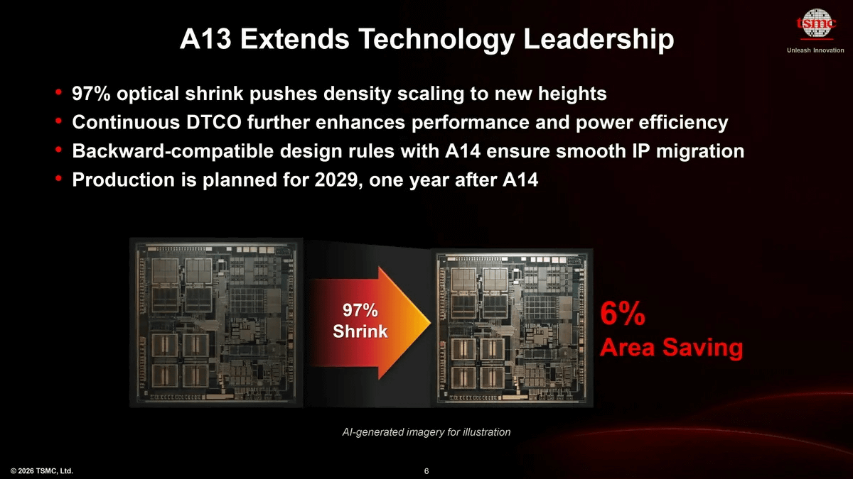
The most prominent product in this announcement was the 'A13.' The A13 is positioned as a 'direct shrink' version of the A14, which was announced in 2025. It features a 6% reduction in area compared to the A14, while maintaining full backward compatibility with the A14's design rules, allowing customers to transition with relatively few redesigns. Furthermore, TSMC's proprietary Design and Manufacturing Co-Optimization (DTCO) technology will improve power efficiency and performance, and mass production is scheduled to begin in 2029, one year after the A14.
The 'A12' is positioned as an enhanced version of the A14 series, employing back-side power supply technology (BSPDN) using Super Power Rail, and is scheduled to begin production in 2029 as a process intended for AI and HPC applications.
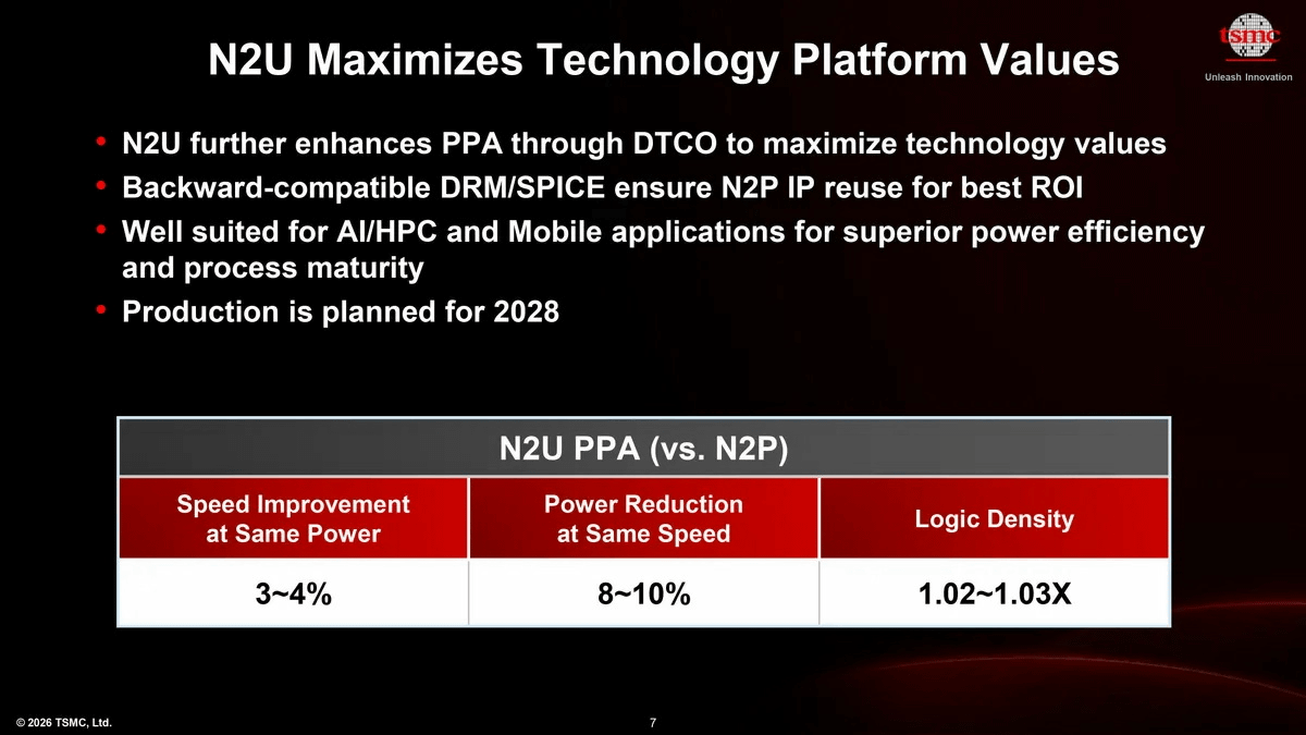
TSMC's 2nm process technology, 'N2U,' is an enhanced version of the 2nm platform that will achieve a 3% to 4% speed improvement, or an 8% to 10% reduction in power consumption at the same speed, as well as a 1.02 to 1.03 times increase in logic density compared to N2P, and is scheduled to begin production in 2028. The aim is to leverage the mature 2nm substrate and yield while maintaining compatibility with N2P IP assets to facilitate investment recovery, and it is described as a balanced option that can be used not only for client applications but also for AI, HPC, and mobile.
On the other hand, the high-performance line for AI data centers will center around the '
TSMC states that 'this roadmap is not only about logic miniaturization, but also about expanding packaging technologies to support the AI era.' TSMC's 2.5D stacked packaging technology, CoWoS, is already being used in 5.5 reticle (approximately 4720 mm² ) products currently in production, and by 2028, they plan to mass-produce 14-reticle (approximately 12,000 mm² ) packages that can integrate around 10 large computing dies and an HBM20 stack. Furthermore, by 2029, they anticipate further expansion to mass-produce 40-reticle (approximately 34,320 mm² ) class SoW-X (SoW-X) integrated circuits.
by
The 'A14-to-A14 SoIC,' scheduled for mass production in 2029, utilizes 3D chip stacking technology and is said to achieve 1.8 times the inter-die I/O density compared to the previous generation 'N2-on-N2 SoIC.' TSMC also reported that its proprietary next-generation copacked optics technology, 'COUPE on substrate,' aimed at accelerating AI in data centers, is scheduled to begin mass production in 2026. TSMC touted that this COUPE on substrate achieves twice the power efficiency and one-tenth the latency compared to detachable optical modules on a substrate.
For automotive and robotics applications, 'N2A' was announced as the first automotive-grade technology to utilize nanosheet transistors. N2A is expected to offer a 15% to 20% speed improvement over N3A at the same power level, and AEC-Q100 certification is scheduled to be completed in 2028. In addition, an 'Auto-Use' design kit will be provided that incorporates automotive usage conditions within the N2P design kit, making it easier to start development even before full certification of N2A is available.
The N3A itself is scheduled to enter production in 2026, and it is said that more than 10 product plans are already underway through the 'Auto Early' program which began in 2023.
In addition, the 'N16HV' for display drivers was also announced. This is positioned as bringing high-voltage technology to the FinFET generation, and is said to increase gate density by 41% and reduce power consumption by 35% compared to TSMC's N28HV. For nearsightedness displays, it is expected to reduce die area by 40% and reduce power consumption by more than 20%, which will also lead to improved usability in applications such as smart glasses.
Tom's Hardware stated that this roadmap 'clearly demonstrates TSMC's two-pronged strategy, not only by advancing the miniaturization of advanced logic, but also by adopting different paces of evolution for client-side and AI/HPC-oriented applications.' By presenting in parallel lines—one that emphasizes the reuse and ease of migration of design assets, such as A13 and N2U, and another that aims to meet the demands of the AI era, including power supply and implementation scale, such as A12 and advanced packaging—this announcement makes it clearer that TSMC's competitive focus until 2029 is not just 'miniaturization,' but also 'the expansion of the entire system, including implementation technology.'
Related Posts:


in Hardware, Posted by log1i_yk