Diamond coating as a heat dissipation material for semiconductors successfully suppresses peak temperatures

Diamond, with its high thermal conductivity, is one of the ideal materials for semiconductors, and after overcoming various obstacles, construction of the world's first
Diamond Thermal Conductivity: A New Era in Chip Cooling - IEEE Spectrum
https://spectrum.ieee.org/diamond-thermal-conductivity
The thermal conductivity of single-crystal diamond is about six times that of copper, making it one of the highest values of any material. Polycrystalline diamond, which is easy to manufacture, can also approach this value by growing it thick. This makes diamond semiconductors attractive, but Professor Srabanti Choudhury of Stanford University, who has been working on gallium nitride device research, said he anticipated significant challenges. For example, while several companies were working on making high-purity diamond substrates 50mm, 75mm, or 100mm thick, Professor Choudhury's team was only able to obtain substrates that were only 3mm thick.
So Professor Chowdhury changed tack: instead of trying to grow commercial-scale diamond substrates, he began trying to grow diamond films on large silicon wafers.
Generally, when methane and hydrogen are reacted at temperatures above 900°C, a large number of thin crystal pillars are formed rather than single crystals. As the height increases, they coalesce into a uniform film, but by the time a high-quality polycrystalline diamond film is formed, the film becomes thick and often develops cracks.
Professor Chowdhury envisioned using this polycrystalline coating as a heat dissipation material in other devices, and saw an opportunity in the idea that diamond, being an electrical insulator, could act as a 'thermal dielectric.'
However, there was not enough space inside the chip to grow the diamond film, and the spiked crystal pillars that appear in the early stages of growth do not conduct heat laterally, so large crystal grains had to be generated from the start. Furthermore, the high temperatures required to grow the diamond film could damage the chip, so the temperature had to be reduced by at least half.
Through trial and error, the team discovered that adding oxygen to the mixture continuously removed the non-diamond carbon deposits, and found a formula that formed a coarse-grained polycrystalline diamond coating all over at 400°C, a temperature that CMOS circuits and other devices can withstand.
However, they faced a challenge ahead: thermal boundary resistance (TBR). TBR is a phenomenon in which heat is less likely to be transmitted at the boundary surface where different crystals come into contact, and in many cases this is overcome by using a different material at the boundary. In the case of semiconductors, the materials available are limited, which limits options.
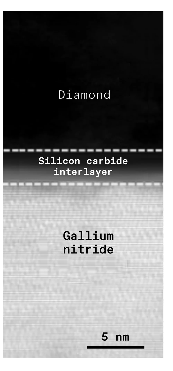
While growing diamond films on gallium nitride (GaN) coated with silicon nitride, Professor Chowdhury's research team accidentally observed a lower TBR than previously reported. In collaboration with K. J. Cho of the University of Texas at Dallas, they discovered that silicon carbide formed at the interface between the diamond and silicon nitride acts as a thermal bridge, resulting in a lower TBR.
by Mohamadali Malakoutian
The research team tested low-TBR diamond coating on gallium nitride high-electron mobility transistors (HEMTs). HEMTs were chosen as a test case because the gate that controls the current is located just a few nanometers from the transistor, generating heat very close to the device's surface, making the effect of diamond coating immediately visible. In fact, when diamond coating was applied completely around the sides of the HEMT, there was some degradation in high-frequency performance, but the temperature dropped by 70 degrees.
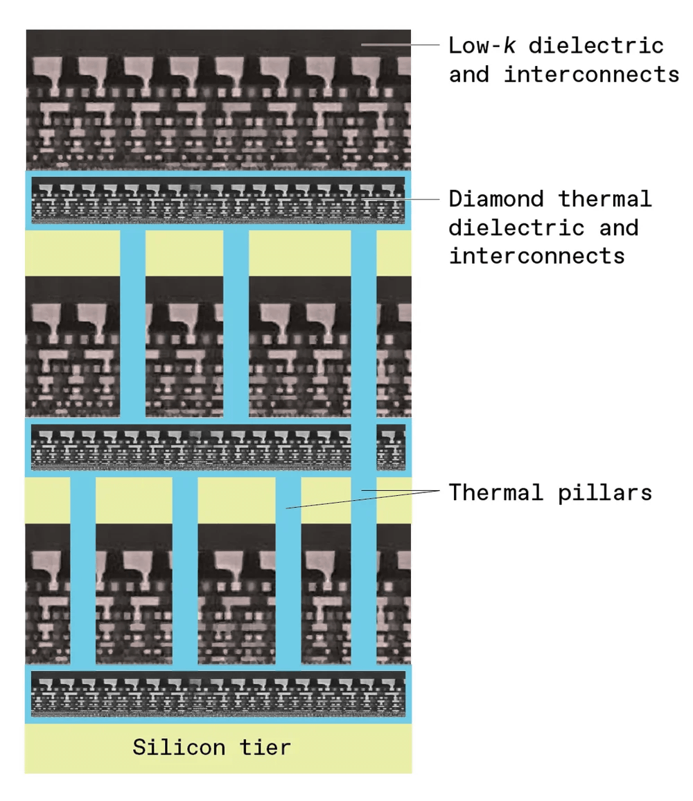
In his work, Professor Chowdhury employs a concept called 'thermal scaffolding.' This involves embedding nanometer-sized layers of polycrystalline diamond within the dielectric layer on top of the transistors to spread heat, with the layers connected by vertical thermal pillars made of copper or diamond. The pillars are then connected to another heat sink, which then leads to the thermal pillars of the next chip in the 3D stack, and the process continues until the heat reaches a heat sink or other cooling device.
by Srabanti Chowdhury
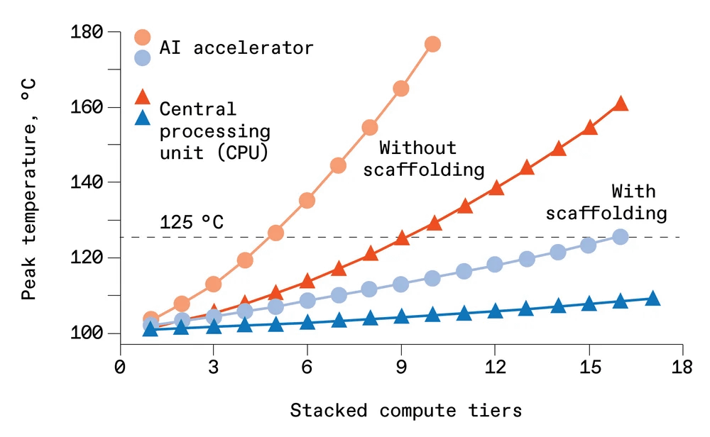
The graph below shows the thermal changes with and without thermal scaffolding for the AI accelerator (circle) and CPU (triangle). The red line shows the results without thermal scaffolding, and the blue line shows the results with thermal scaffolding. With thermal scaffolding, the peak temperature is kept to 125°C.
by Srabanti Chowdhury
While there are still challenges ahead, such as figuring out how to make the top of the diamond coating atomically flat, Professor Chowdhury says the research represents a 'disruptive' new avenue for thermal management and could be an important step towards the future of high-performance computing.
Related Posts: