An expert explains in an easy-to-understand way what CPU cache memory is
When talking about CPU specifications, in addition to clock speed and number of cores/threads, ' CPU cache memory ' is sometimes mentioned. Developer Gabriel G. Cunha explains what this CPU cache memory is.
Pikuma: Exploring How Cache Memory Really Works
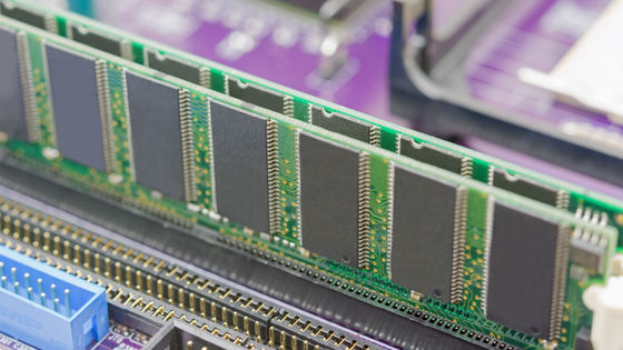
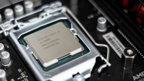
Cache memory is located between the CPU and main memory (RAM) and exists to bridge the speed gap between the two. Because the processing speed of the CPU has become significantly faster than the access speed of RAM, frequently used data can be temporarily stored in the high-speed cache, reducing the time the CPU has to pause processing while waiting for data.
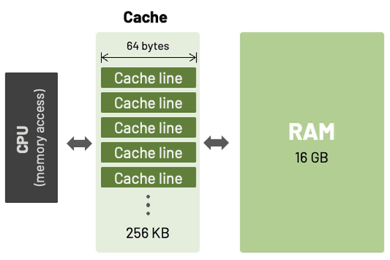
Data from RAM is read into the cache in blocks called 'cache lines', the size of which varies depending on the processor architecture, but is commonly 32, 64, or 128 bytes.
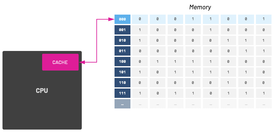
When the data the CPU needs is in the cache, it is called a 'cache hit,' which allows for fast access. Conversely, when the data is not in the cache and needs to be read from RAM, it is called a 'cache miss,' which leads to reduced performance. Therefore, programmers need to be aware of increasing the cache hit rate and reducing cache misses.
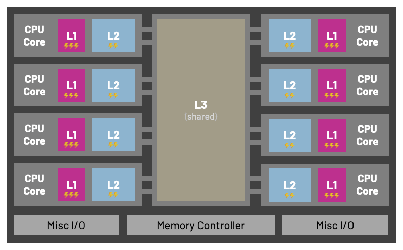
Modern CPU caches typically consist of multiple levels: L1, L2, and L3.
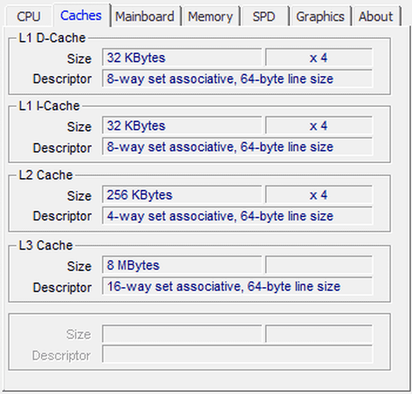
・L1 cache
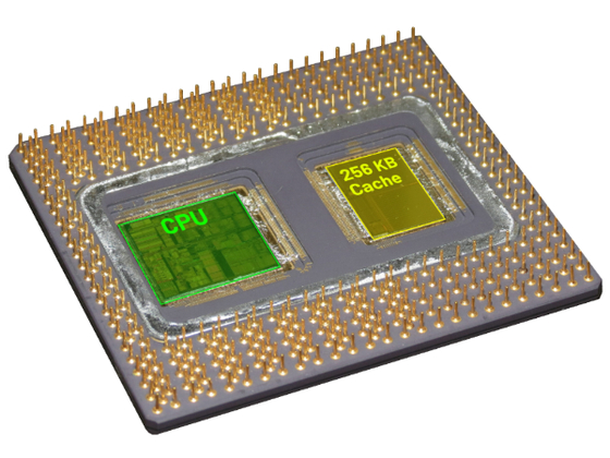
It is closest to the CPU core and is fast, but its capacity is quite small, at only a few tens of KB. L1 cache is often separated into a data cache (d-cache) for data processed by programs, and an instruction cache (i-cache) for storing instructions such as assembly code. For example, the Intel Pentium, which was released in 1993, had 8 KB of L1 cache memory for data cache and instruction cache.
・L2 cache
L2 cache is slower than L1 cache, but has a larger capacity of several hundred KB. The Pentium Pro, introduced in 1995, was the first Intel x86 processor to have an L2 cache, with a capacity of 256 KB or 512 KB.
・L3 cache
L3 cache is the slowest but largest cache memory, with a capacity of several MB, and is typically shared by multiple CPU cores.
The data cache stores data and therefore supports both reads and writes, but the instruction cache is rarely rewritten during execution, so it basically functions as read-only. Because the access characteristics of the data cache and the instruction cache are different, separating their roles allows for the creation of a more efficient cache system.
Modern architectures have separate instruction and data caches. Most ARM CPUs have separate instruction and data caches in L1, but they are combined in L2.
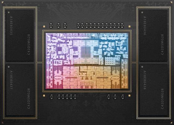
For example, the instruction cache and data cache are separate in the Apple Silicon M1 and M2. The M2 CPU has two types of cores: high-performance and high-efficiency. The high-performance core has a 192KB L1 instruction cache, a 128KB L1 data cache, and a 16MB L2 cache. On the other hand, the high-efficiency core has a 192KB L1 instruction cache, a 64KB L1 data cache, and a 4MB L2 cache.
A cache has the property of loading all the data surrounding the data it has loaded once, so it is important to place the data used in processing as close to each other as possible in memory.
For example, when processing a two-dimensional array in C, since C arrays are stored in memory in row-major order, processing columns in an inner loop and rows in an outer loop will result in much higher cache efficiency. This is because consecutive data in memory is accessed sequentially, improving the cache hit rate.
[code]int sum_matrix_rows(int mat[M][N]) {
int sum = 0;
for (int i = 0; i < M; i++) {
for (int j = 0; j < N; j++) {
sum += mat[i][j];
}
}
return sum;
}[/code]
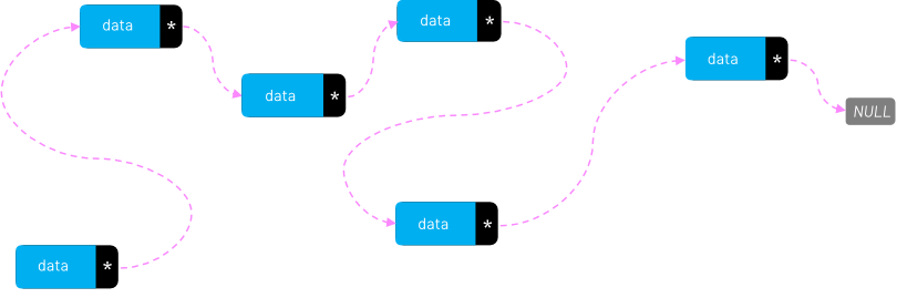
Conversely, a linked list, whose elements tend to be scattered across memory, is an inefficient data structure from a cache perspective.
'We hope that this new knowledge about how computer memory works and how it works in conjunction with the CPU will help us gain a deeper understanding of cache operations,' Cunha said.
Related Posts:

in Hardware, Posted by log1i_yk