Nintendo Switch 2 SoC analysis reveals eight A78C cores, 1536 Ampere shaders, and Samsung's 8nm process, with performance comparable to the GTX 1050 Ti
YouTuber Geekerwan has obtained a
This is Nintendo Switch 2's CPU! - YouTube
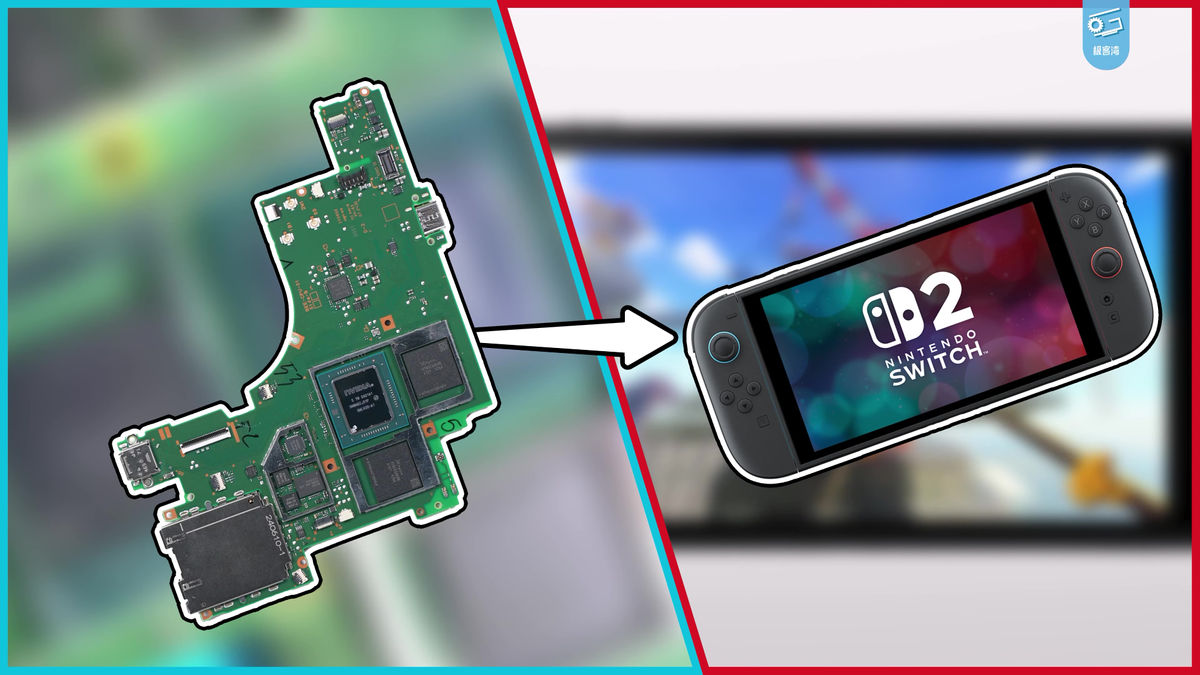
According to Geekerwan, the motherboard that is said to be for the Nintendo Switch 2 was being sold on the Chinese e-commerce site Xianyu. He decided to buy it because the photo on the sales page matched the photo of the Nintendo Switch 2 motherboard that had been leaked .
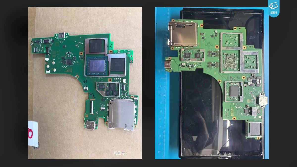
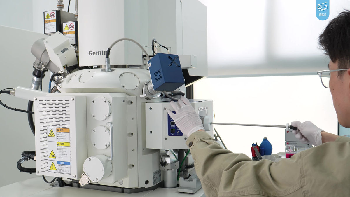
After obtaining the motherboard, Geekerwan analyzed the accessories using an IR (infrared) microscope and a FIB-SEM (focused ion beam scanning electron microscope).
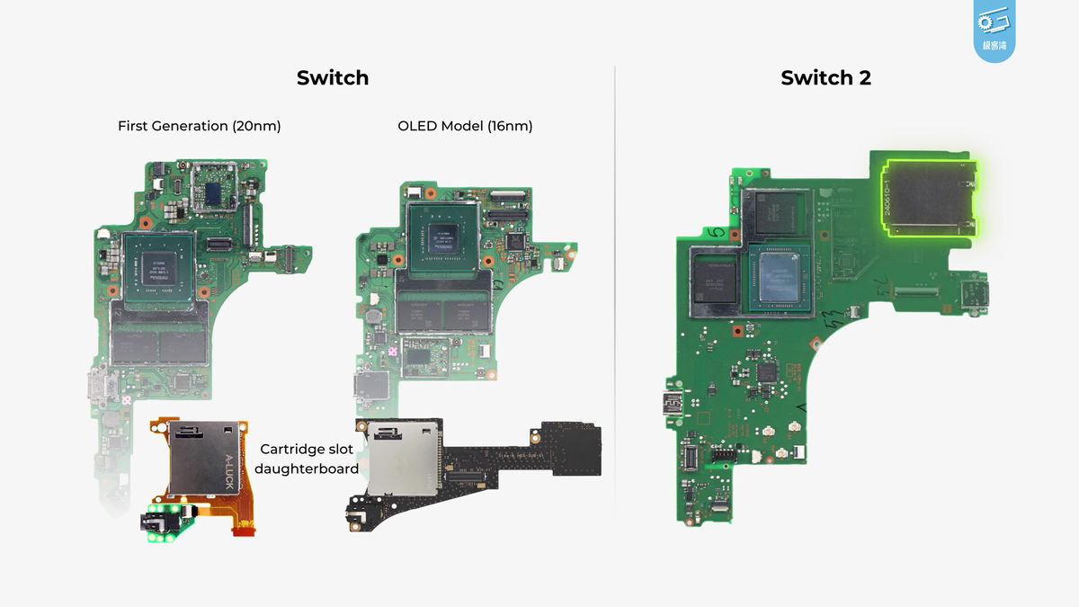
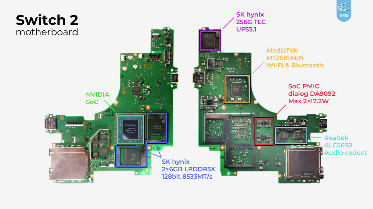
First of all, the size. The Nintendo Switch 2 motherboard is slightly larger than
Next, we will look at the details of each part. The SoC is manufactured by NVIDIA and is equipped with Hynix 256GB TLC UFS 3.1 storage, MediaTek's MT3681AEN Wi-Fi/Bluetooth chip, Realtek's ALC5658 audio chip, and a two-phase PMIC (power management IC) that supplies power to the SoC. Note that the maximum power supply of the PMIC is 34.4W, but Geekerwan points out that the power consumption of the SoC itself is much less. The DRAM is two Hynix 6GB LPDDR5X 128bit 8533MT/s, for a total of 12GB.
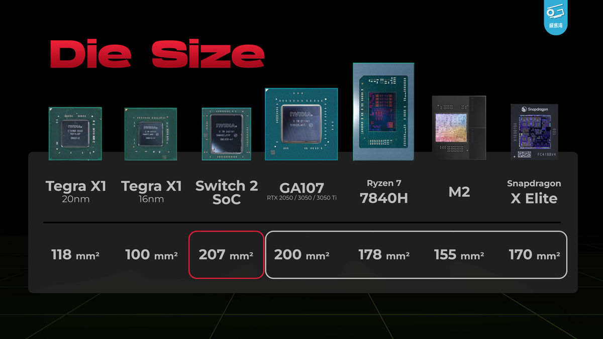
The die size of the SoC is 207 square millimeters, almost twice the size of the Nintendo Switch (118 square millimeters) and the Nintendo Switch (OLED model) (100 square millimeters). It is larger than the GA107 used in the NVIDIA RTX 3050 and the Apple M2.
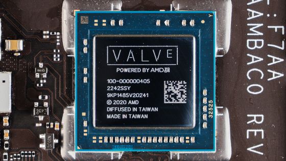
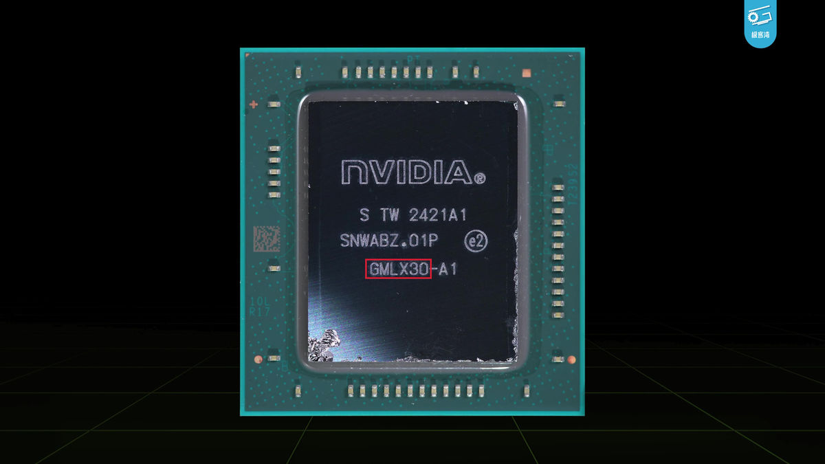
The engravings reveal that the SoC is of type GMLX30-A1, is manufactured by Samsung, and was packaged in Taiwan in the 21st week of 2024.
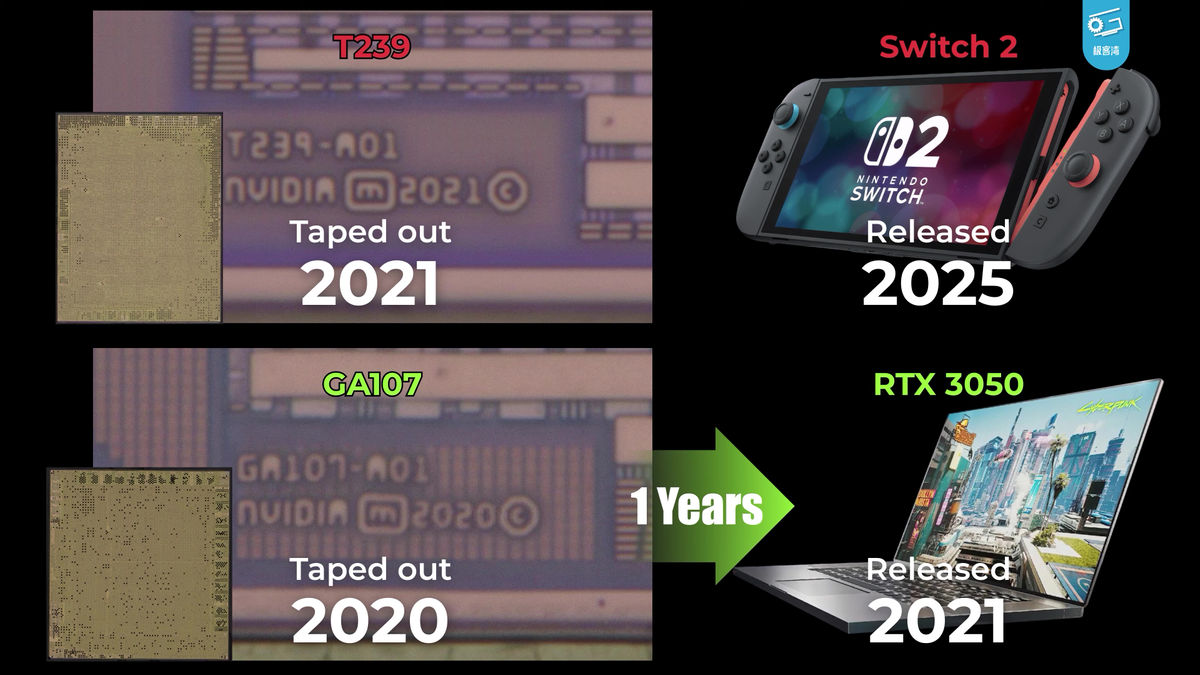
Further examination under a microscope revealed that the metal surface was engraved with T239. The engraving was done in 2021, suggesting that there was a four-year time lag between the development of the chip and the release of the Nintendo Switch 2. Geekerwan points out that this 'confirms the rumors that it was supposed to be released earlier but was delayed.'
The T239 is a custom chip made by NVIDIA. The CPU and GPU are arranged like this.
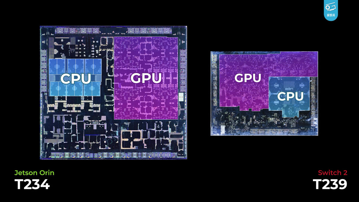
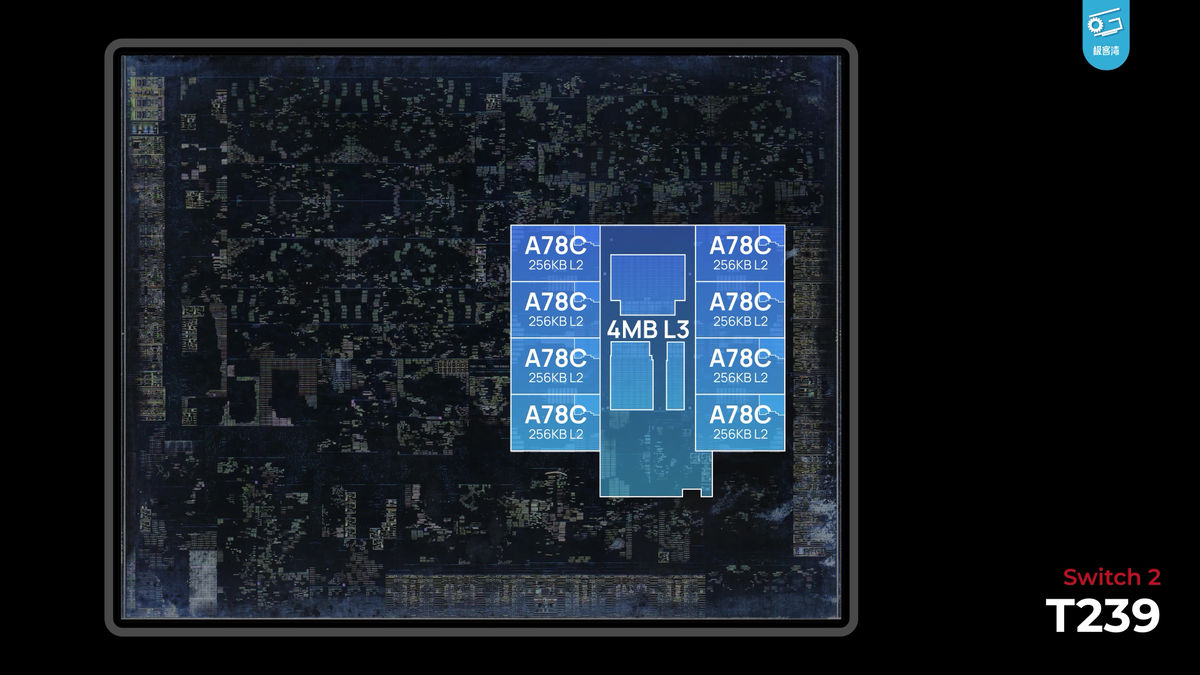
The CPU is packed with eight A78C CPUs, each with its own 256K L2 cache and a central 4MB L3 cache, and the A78C cores are said to be the exact same size as the A78AE cores in Orin, which uses Samsung's 8nm process.
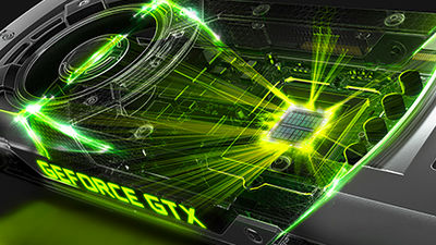
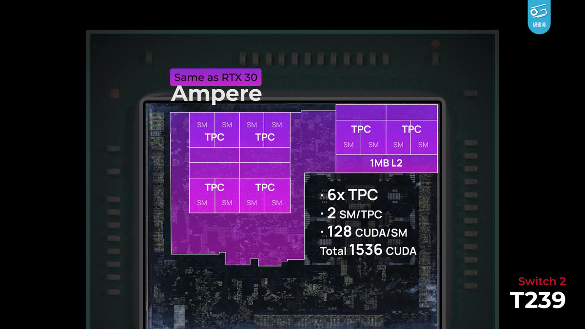
Surrounding the CPU is the GPU. It uses NVIDIA's Ampere architecture, which is also used in NVIDIA's RTX 30 series, and has six
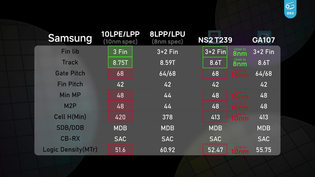
When the T239 transistors were examined using FIB-SEM, it was found that there were some commonalities with chips manufactured using the 10nm process in parts such as the gate pitch of the transistors, but there were also some commonalities with chips manufactured using the 8nm process. 'The T239 is a mix of 10nm and 8nm. Samsung's 8nm process (Samsung 8N) refers to a process based on 10nm with 8nm fine-tuning, so the T239 is equivalent to 8N,' Geekerwan said.
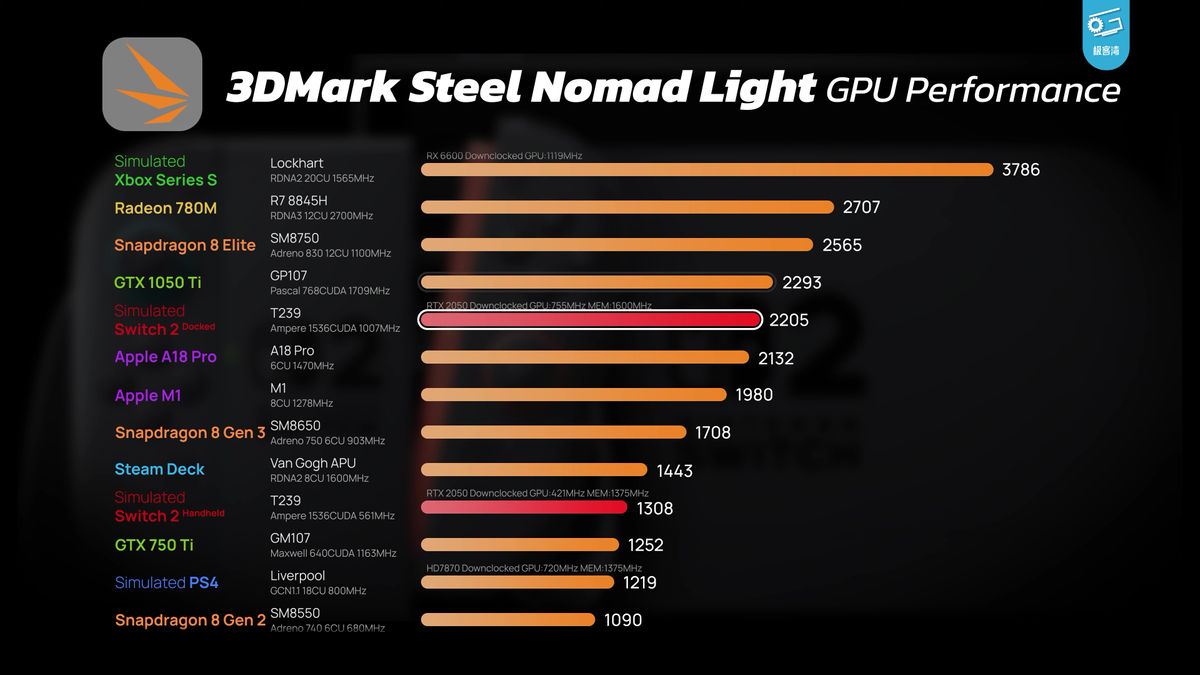
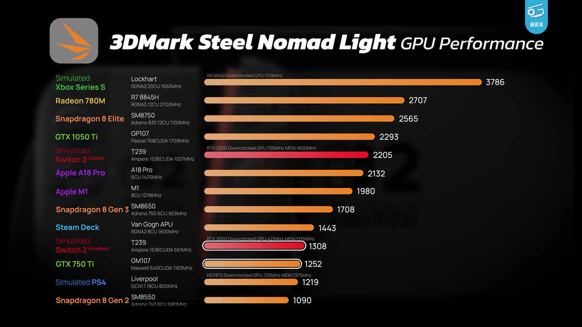
Geekerwan also estimated the performance of the Nintendo Switch 2. When the Nintendo Switch 2 is docked in TV mode, the estimated performance based on the 3DMark Steel Nomad Light benchmark is higher than the Apple A18 Pro and lower than the GTX 1050 Ti.
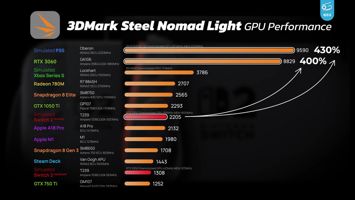
The PlayStation 5 home console and the RTX 3060 desktop PC GPU deliver four times the performance of the Nintendo Switch 2.
In portable mode, it is equivalent to a GTX 750 Ti, which is slightly faster than the PlayStation 4. It is at a similar level to the '
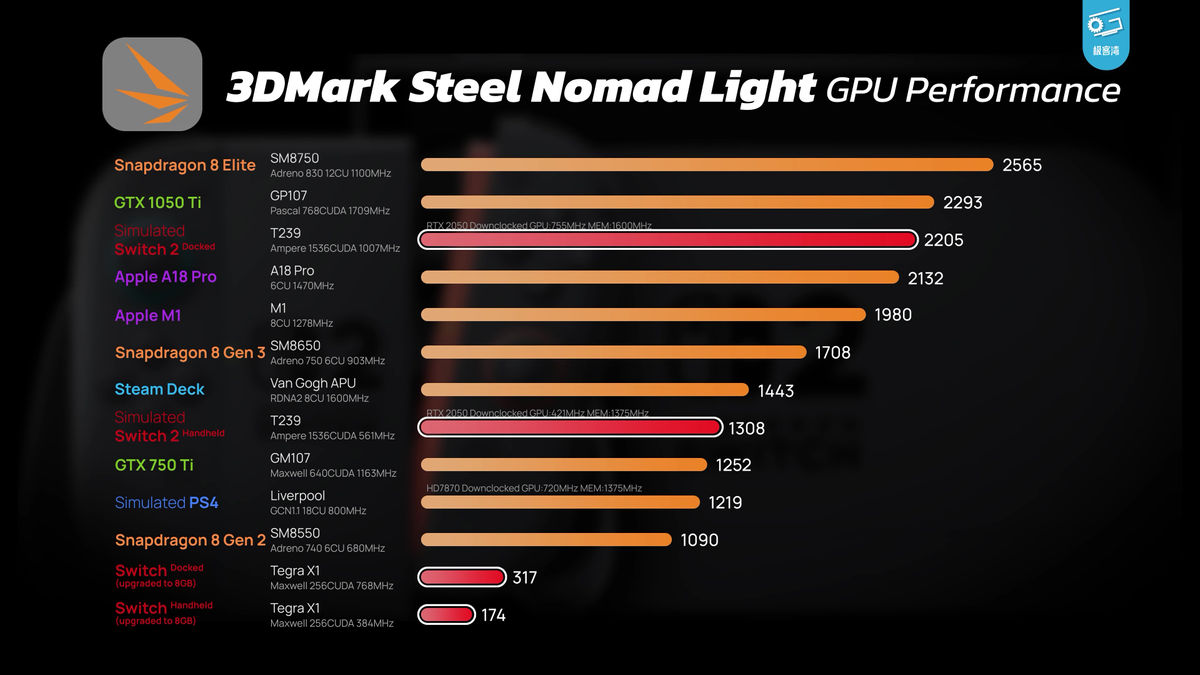
It is a huge improvement over the NVIDIA Tegra X1 used in the Nintendo Switch.
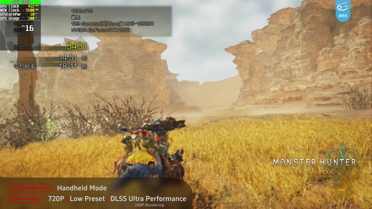
However, it seems to have difficulty running AAA games, and when simulating 'Monster Hunter Wilds' played in TV mode, the FPS is apparently less than 30.
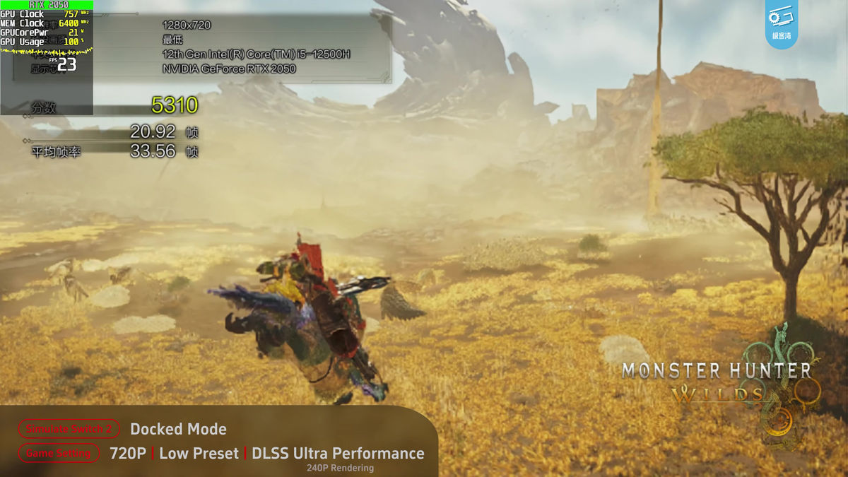
In handheld mode, the performance is lower and the graphics are worse, but if these titles are released for the Nintendo Switch 2, they will likely be optimized accordingly.
Related Posts: