Reverse Engineering SanDisk's High Endurance microSD Card
SanDisk sells
Reverse-engineering and analysis of SanDisk High Endurance microSDXC card | Rip It Apart – Jason's electronics blog-thingy
https://ripitapart.com/2020/07/16/reverse-engineering-and-analysis-of-sandisk-high-endurance-microsdxc-card/
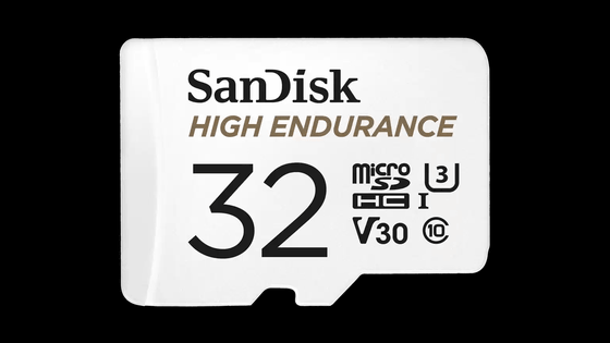
Drive recorders and security cameras are constantly recording video, so the microSD cards used to store the media are constantly writing and rewriting data. This puts a heavy load on the SD card, but SanDisk's 'SanDisk High Endurance microSD Card' boasts that it can withstand such high-load tasks.
Gin was interested in the SanDisk High Endurance microSD Card, but because SanDisk does not disclose detailed specifications about the internal operation of SD cards, he had no way of finding out the details other than through reverse engineering.
Gin emailed SanDisk's support team to ask about the type of NAND flash memory used in the lineup of SD cards that boast high durability, as well as durability indicators such as P/E cycles (program/erase cycles) and total write capacity (TBW). SanDisk's support team explained that they could not provide information that was not included in the published specifications, but responded that 'all cards use MLC (flash memory that can store two bits per cell).'
Gin explains that while microSD cards seem like a robust, monolithic piece of technology, they're actually made up of several different chips, each with a different role to play: Essentially, an SD card consists of a controller to manage the NAND flash memory and communicate with the host (the device into which the SD card is inserted, such as a PC or camera), and the NAND flash memory itself.
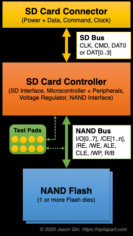
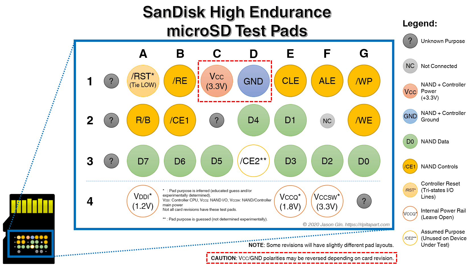
microSD cards often include a test pad during manufacturing to program and test the NAND Flash memory. Although the test pad can be misused for data recovery, it can also be used to convert microSD cards with faulty controllers or firmware to raw NAND Flash data for reuse. However, there is no standard for this test pad.
microSD cards fall into the category of monolithic flash devices, combining a controller and NAND flash memory in a single, inseparable package. Many manufacturers split off the data bus of their flash devices into hidden test pads, allowing other SD card and USB drive manufacturers to produce cheaper storage devices by repurposing failed parts.
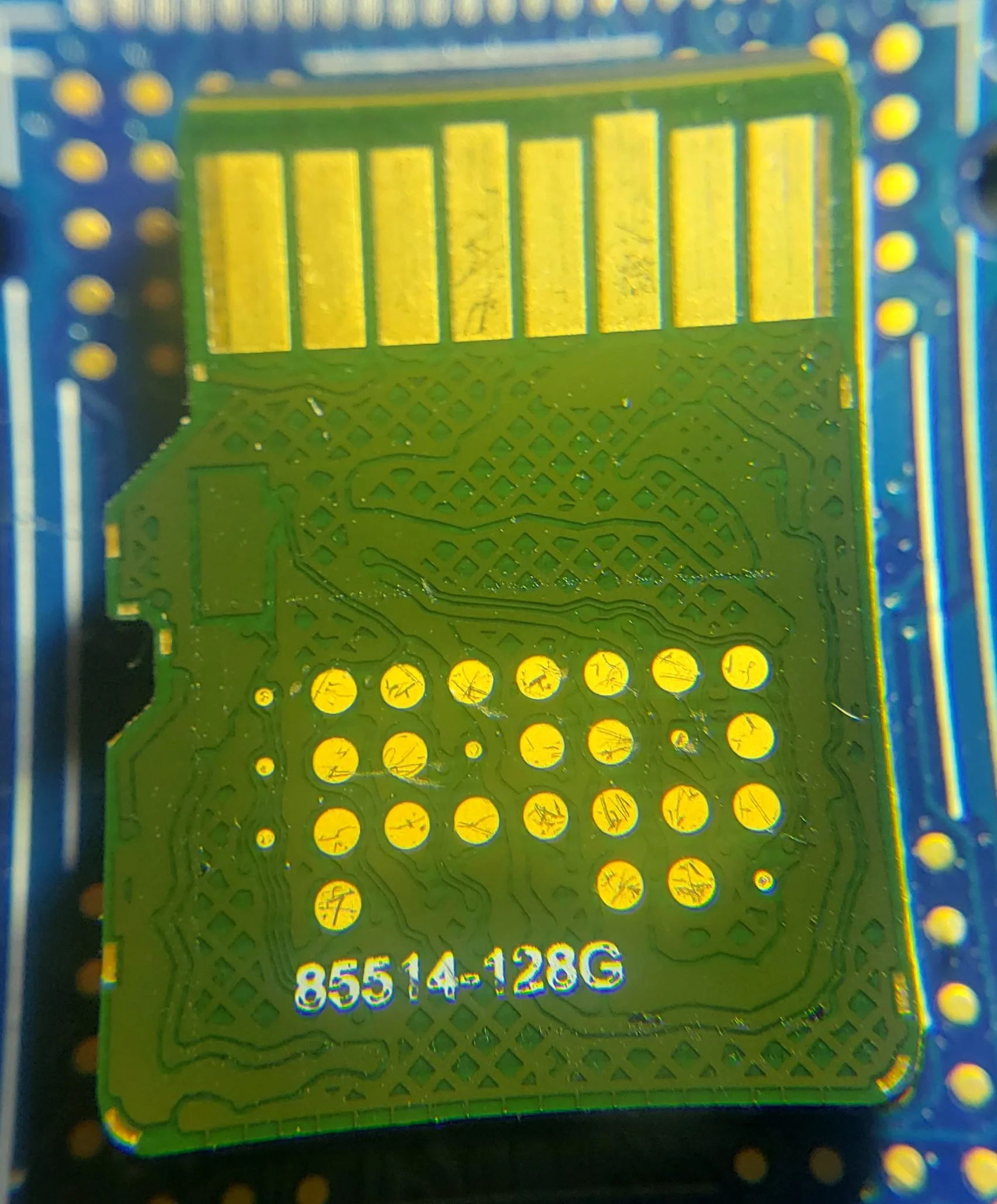
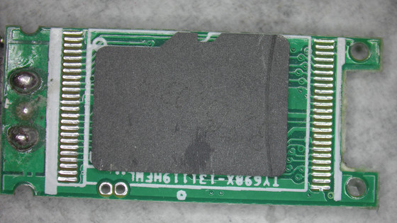
SanDisk has very limited information on the pinout of the test pad on their SD cards, but the layout is said to be nearly the same with slight variations from generation to generation. The SanDisk High Endurance microSD Card features a test pad that is not covered by solder mask, and instead has the serial number laser etched on it.
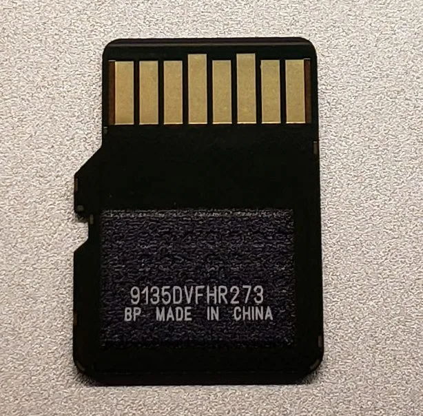
Therefore, it seems that the coating on the test pad can be easily removed by applying a little heat and rubbing. Once the coating is removed, the layout of the test pad appears as shown below.
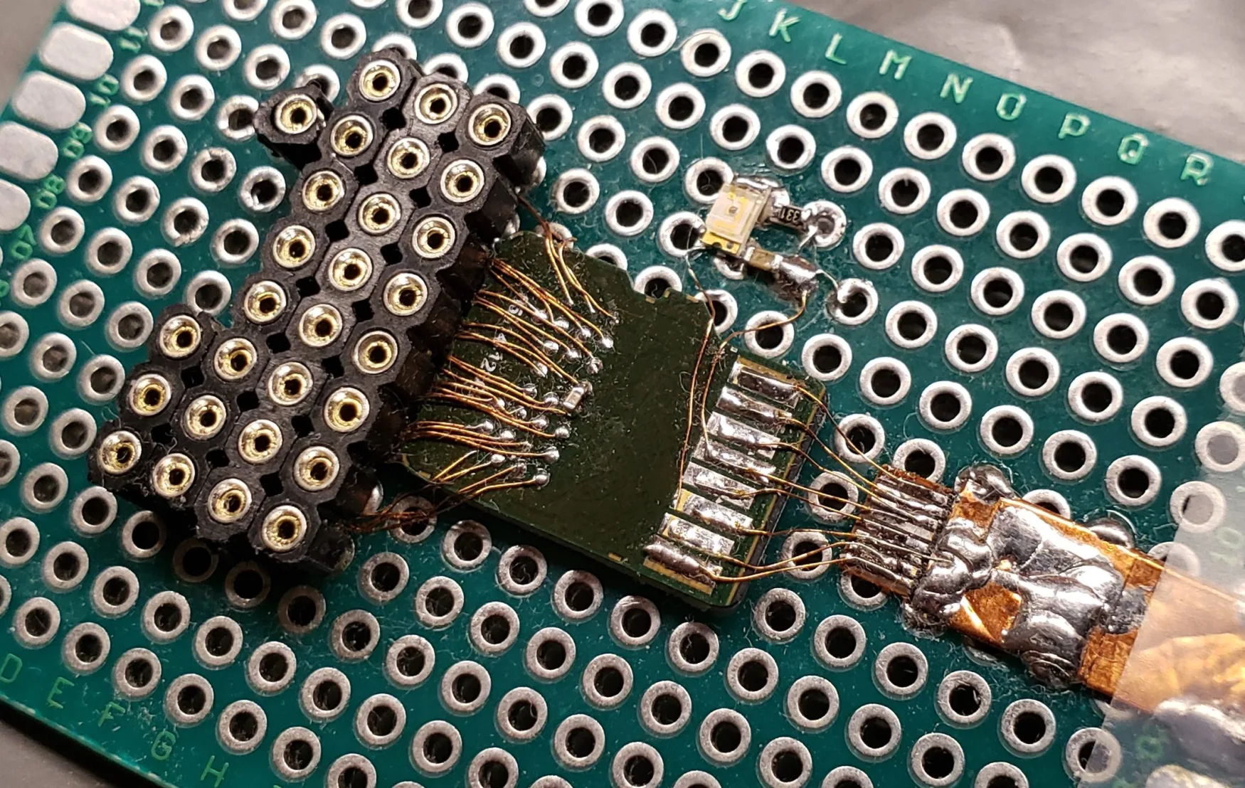
A breakout board is constructed to allow easy access to each test pad.
Gin used a USB-based logic analyzer,
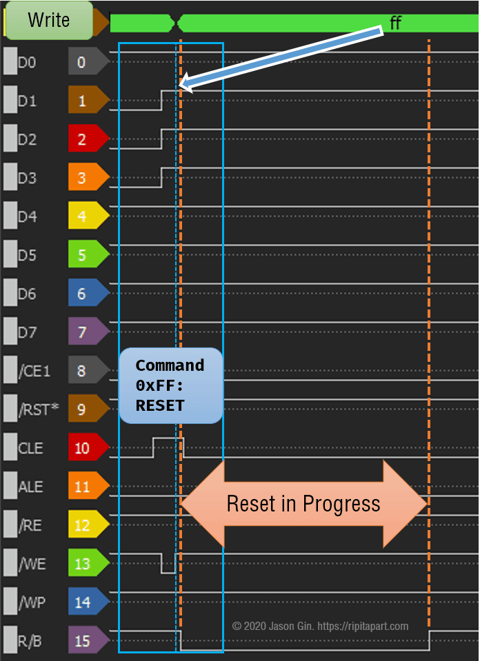
'We were looking for two commands: RESET (0xFF) and READ ID (0x90),' Gin explains. 'When looking for a command sequence, it's important to know how and when the data and control lines change.' Below is a logic analyzer trace of the RESET command. The dotted lines show where the write and reset occur.
Below is a logic analyzer trace of a READ ID command, the dotted lines show where the read/write occurs.
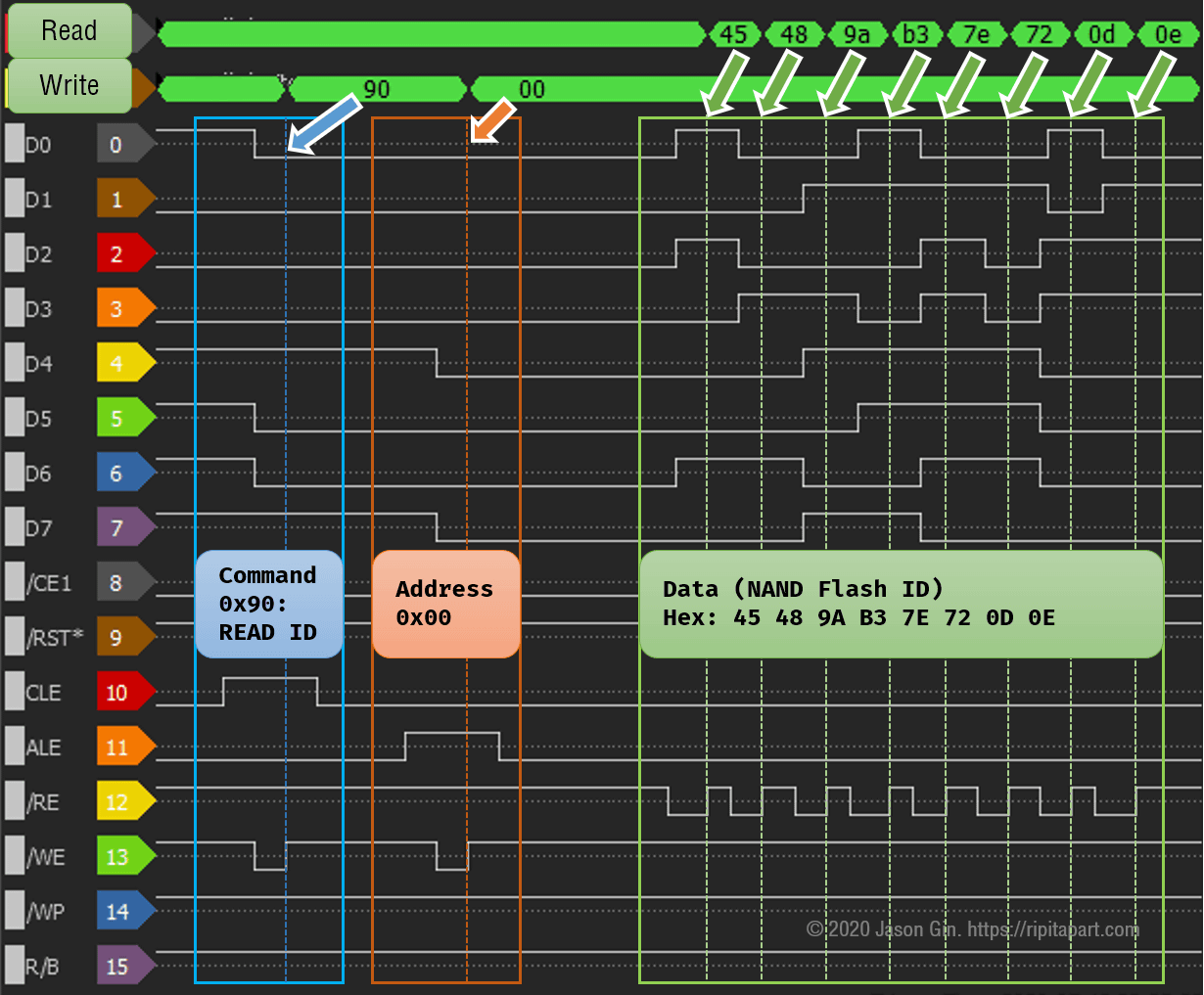
Each NAND flash memory has a unique ID to identify the manufacturer and other functional data defined by the manufacturer. The first byte represents the manufacturer of the flash memory, and the remaining bytes (2-6 bytes) define the characteristics of the device as set by the manufacturer. Most NAND flash memory vendors are tight-lipped about their datasheets, and SanDisk and Toshiba (Kioxia) seem to keep them very tight-lipped, except for a slightly old
For the 128GB model of the 'SanDisk High Endurance microSD Card', the ID of the NAND flash memory is '0x45 48 9A B3 7E 72 0D 0E'. '45' indicates that 'the manufacturer is SanDisk', and the next '48' is presumed to indicate 'I/O voltage and device capacity'. '9A' indicates 'NAND flash memory type: TLC, number of flash dies per /CE: 4', 'B3' indicates 'block size is 12MiB, page size is 16,384 bytes (16kiB) excluding the spare area', '7E' indicates 'number of planes per /CE: 8', and '72' indicates 'interface type: asynchronous, process geometry: BiCS3 3D NAND'. However, the details of the remaining '0D' and '0E' were not known.
From these information, it is clear that the 'SanDisk High Endurance microSD Card' uses a NAND flash memory called BiCS3 3D TLC, which is a 3D NAND with significantly improved endurance compared to conventional planar NAND flash memory. However, it was not clear whether the controller utilizes an SLC cache mechanism for write operations.
To verify that he was getting the correct ID from the NAND Flash memory, Gin used a Texas Instruments development board, the MSP-EXP430FR2433 , and wrote some basic code to send the necessary RESET and READ ID commands, extracting some extra data from the JEDEC parameter page that is hidden on the chip in the process.
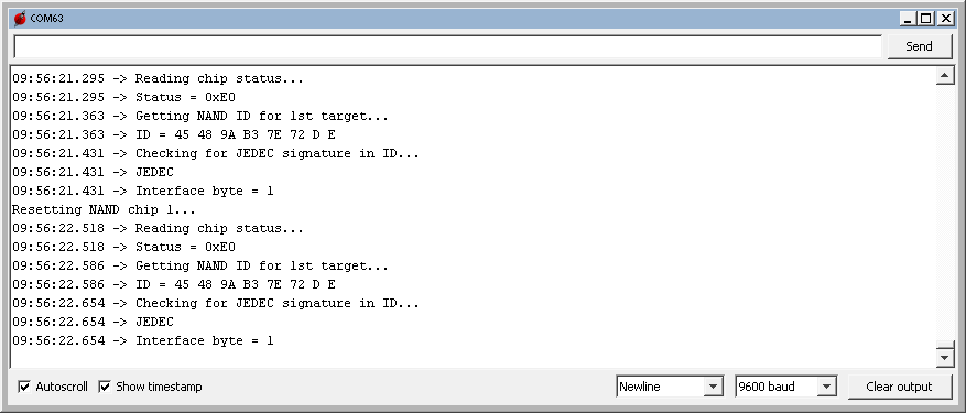
The JEDEC parameter page contained much more detailed characteristic information than was found in the NAND flash memory ID. The JEDEC parameter page was well standardized and much easier to analyze. However, SanDisk ignored the standard format of the JEDEC parameter page and wrote the parameter page in its own way. For example, the JEDEC parameter page usually begins with the ASCII string 'JEDEC', but the 'SanDisk High Endurance microSD Card' appears to have the SanDisk-representing string 'SNDK' repeatedly.
'I was initially confused when trying to find the ID from the logic capture alone,' Gin wrote. 'I spoke to a contact who has experience recovering data from NAND flash memory, and he told me that this is to be expected with SanDisk products, which make heavy use of vendor-specific commands and data structures. If you believe the fourth byte, it says the block size is 4MB, which seems reasonable for modern flash devices. Other than the first byte, which identifies the chip as Toshiba, the rest of the information made absolutely no sense to me.'
'We don't need to do this level of hardware reverse engineering to answer the simple question of what kind of flash SanDisk uses in its high-endurance cards. It would be strange to think that SanDisk would brag about using 3D NAND for its high durability and reliability, when in fact they don't,' he wrote.
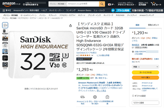
The SanDisk High Endurance microSD Card is also available on Amazon.co.jp, with the 32GB model being sold for 1,293 yen including tax.
Amazon.co.jp: [SanDisk Genuine Product] SanDisk microSD Card 32GB UHS-I U3 V30 Class10 Dash Cam Surveillance Camera High Endurance SDSQQNR-032G-GH3IA Simple Design Package 2 Year Limited Warranty: Computers & Peripherals
Related Posts:


in Hardware, Posted by logu_ii